NNDK-MOD5272-KIT NetBurner Inc, NNDK-MOD5272-KIT Datasheet - Page 444
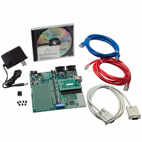
NNDK-MOD5272-KIT
Manufacturer Part Number
NNDK-MOD5272-KIT
Description
KIT DEVELOP NETWORK FOR MOD5272
Manufacturer
NetBurner Inc
Series
ColdFire®r
Datasheets
1.MOD5272-100IR.pdf
(2 pages)
2.MOD5272-100IR.pdf
(550 pages)
3.NNDK-MOD5282-KIT.pdf
(2 pages)
Specifications of NNDK-MOD5272-KIT
Main Purpose
*
Embedded
*
Utilized Ic / Part
MOD5272
Primary Attributes
*
Secondary Attributes
*
Processor To Be Evaluated
MOD5272
Interface Type
RS-232, RS-485, USB
Lead Free Status / RoHS Status
Contains lead / RoHS non-compliant
Lead Free Status / RoHS Status
Lead free / RoHS Compliant, Contains lead / RoHS non-compliant
Other names
528-1001


Queued Serial Peripheral Interface (QSPI) Signals
19.15 Queued Serial Peripheral Interface (QSPI)
This section describes signals used by the queued serial peripheral interface (QSPI)
module. Four QSPI chip selects, QSPI_CS[3:0], are multiplexed with the physical layer
interface pins and GPIO port A. QSPI_CS0 is always available. QSPI_CS3 is multiplexed
with DOUT3 and PA7.
19.15.1 QSPI Synchronous Serial Data Output
The QSPI synchronous serial data output (QSPI_Dout) can be programmed to be driven on
the rising or falling edge of SCK. Each byte is sent msb first.
WSEL configuration input is sampled on the rising edge of Reset Output (RSTO).
19.15.2 QSPI Synchronous Serial Data Input (QSPI_Din)
The QSPI synchronous serial data input (QSPI_Din) can be programmed to be sampled on
the rising or falling edge of QSPI_CLK. Each byte is written to RAM lsb first.
19.15.3 QSPI Serial Clock (QSPI_CLK/BUSW1)
The QSPI serial clock (QSPI_CLK/BUSW1) provides the serial clock from the QSPI. The
polarity and phase of QSPI_CLK are programmable. The output frequency is programmed
according to the following formula, in which n can be any value between 1 and 255:
At reset, QSPI_CLK/BUSW1 is used to configure the width of memory connected to CS0.
BUSW1 configuration input is sampled on the rising edge of Reset Output (RSTO).
19.15.4 Synchronous Peripheral Chip Select 0
The synchronous peripheral chip select 0 (QSPI_CS0) output provides a QSPI peripheral
chip select that can be programmed to be active high or low. During reset, this pin is used
to configure the width of memory connected to CS0.
BUSW0 configuration input is sampled on the rising edge of Reset Output (RSTO).
19-30
Signals
QSPI_CLK = CLKIN/(2 × n)
(QSPI_Dout/WSEL)
(QSPI_CS0/BUSW0)
MCF5272 User’s Manual
MOTOROLA
Related parts for NNDK-MOD5272-KIT
Image
Part Number
Description
Manufacturer
Datasheet
Request
R

Part Number:
Description:
BOARD SERIAL-ETHERNET 512K FLASH
Manufacturer:
NetBurner Inc
Datasheet:

Part Number:
Description:
PROCESSOR MODULE FLASH MOD5272
Manufacturer:
NetBurner Inc
Datasheet:

Part Number:
Description:
PROCESSOR MODULE 512KB FLASH
Manufacturer:
NetBurner Inc
Datasheet:

Part Number:
Description:
DUAL PORT SERIAL-ETHERNET
Manufacturer:
NetBurner Inc
Datasheet:

Part Number:
Description:
PROCESSOR MODULE FLASH
Manufacturer:
NetBurner Inc
Datasheet:

Part Number:
Description:
PROCESSOR MODULE 512KB FLASH
Manufacturer:
NetBurner Inc
Datasheet:

Part Number:
Description:
MOD5234 10/100 ETHERNET MODULE
Manufacturer:
NetBurner Inc
Datasheet:

Part Number:
Description:
KIT DEVELOP NETWORK FOR MOD5282
Manufacturer:
NetBurner Inc
Datasheet:

Part Number:
Description:
DUAL PORT SERIAL-ETHERNET
Manufacturer:
NetBurner Inc
Datasheet:

Part Number:
Description:
Ethernet Modules & Development Tools 32 Bit 66MHz 40 Pin DIP Industrial Temp
Manufacturer:
NetBurner Inc
Datasheet:

Part Number:
Description:
Ethernet Modules & Development Tools MOD5213 DEVELOPMENT KIT
Manufacturer:
NetBurner Inc

Part Number:
Description:
Ethernet Modules & Development Tools DUAL PORT SERIAL EHTERNET DEVICE
Manufacturer:
NetBurner Inc
Datasheet:

Part Number:
Description:
Ethernet ICs 32bit 147MHz CAN-to- Ethnt Device IndTemp
Manufacturer:
NetBurner Inc
Datasheet: