NNDK-MOD5272-KIT NetBurner Inc, NNDK-MOD5272-KIT Datasheet - Page 299
NNDK-MOD5272-KIT
Manufacturer Part Number
NNDK-MOD5272-KIT
Description
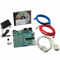
KIT DEVELOP NETWORK FOR MOD5272
Manufacturer
NetBurner Inc
Series
ColdFire®r
Datasheets
1.MOD5272-100IR.pdf
(2 pages)
2.MOD5272-100IR.pdf
(550 pages)
3.NNDK-MOD5282-KIT.pdf
(2 pages)
Specifications of NNDK-MOD5272-KIT
Main Purpose
*
Embedded
*
Utilized Ic / Part
MOD5272
Primary Attributes
*
Secondary Attributes
*
Processor To Be Evaluated
MOD5272
Interface Type
RS-232, RS-485, USB
Lead Free Status / RoHS Status
Contains lead / RoHS non-compliant
Lead Free Status / RoHS Status
Lead free / RoHS Compliant, Contains lead / RoHS non-compliant
Other names
528-1001


MOTOROLA
The MCF5272 PLIC provides two sets of D-channel arbitration control pins:
Because pin set 1 connects ports 1, 2, and 3, these ports do not have D-channel arbitration
control signals.
13.2 GCI/IDL Block
This section describes the GCI/IDL block.
13.2.1 GCI/IDL B- and D-Channel Receive Data Registers
• Port 2: Connects through pin set 1. Operates as a slave-only port. Port 2 shares a data
• Port 3: Connects through pin set 1 or 3. Operates as a slave-only port. Port 3 shares
• DREQ0 and DGNT0 for pin set 0
• DREQ1 and DGNT1 for pin set 1
Demultiplexing
Circuitry
D
IN
clock with port 1: DCL1 when port 1 is in slave mode or GDCL when port 1 is in
master mode. A delayed frame sync, DFSC2, derived from FSC1, is connected to
the DFSC2 output and fed to the port 2 IDL/GCI block. Users can synchronize the
port 2 IDL/GCI block with an offset frame sync, (offset with respect to the port 1
GCI/IDL block), by programming the port 2 sync delay register, P2SDR.
a data clock with port 1: DCL1 when port 1 is in slave mode, or GDCL, when port 1
is in master mode. A delayed frame sync, DFSC3, is derived from FSC1 and is fed
to the port 3 IDL/GCI block. Programming the port 3 sync delay register, P3SDR,
allows it to be synchronized with an offset frame sync (offset with respect to the
port 1 GCI/IDL block). Port 3 can also have dedicated data in and data out pins,
DIN3 and DOUT3 of pin set 3 (see Section 13.5.7, “Port Configuration Registers
(P0CR–P3CR)”). This allows the MCF5272 to connect to ISDN NT1s that have a
common frame sync and clock, but two sets of serial data-in and data-out pins.
DCL
B1 Shift Register
B1 Channel
Chapter 13. Physical Layer Interface Controller (PLIC)
Figure 13-2. GCI/IDL Receive Data Flow
32
Internal Bus
B2 Shift Register
B2 Channel
32
D Shift Register
D Channel
8
GCI/IDL Block
13-3
Related parts for NNDK-MOD5272-KIT
Image
Part Number
Description
Manufacturer
Datasheet
Request
R

Part Number:
Description:
BOARD SERIAL-ETHERNET 512K FLASH
Manufacturer:
NetBurner Inc
Datasheet:

Part Number:
Description:
PROCESSOR MODULE FLASH MOD5272
Manufacturer:
NetBurner Inc
Datasheet:

Part Number:
Description:
PROCESSOR MODULE 512KB FLASH
Manufacturer:
NetBurner Inc
Datasheet:

Part Number:
Description:
DUAL PORT SERIAL-ETHERNET
Manufacturer:
NetBurner Inc
Datasheet:

Part Number:
Description:
PROCESSOR MODULE FLASH
Manufacturer:
NetBurner Inc
Datasheet:

Part Number:
Description:
PROCESSOR MODULE 512KB FLASH
Manufacturer:
NetBurner Inc
Datasheet:

Part Number:
Description:
MOD5234 10/100 ETHERNET MODULE
Manufacturer:
NetBurner Inc
Datasheet:

Part Number:
Description:
KIT DEVELOP NETWORK FOR MOD5282
Manufacturer:
NetBurner Inc
Datasheet:

Part Number:
Description:
DUAL PORT SERIAL-ETHERNET
Manufacturer:
NetBurner Inc
Datasheet:

Part Number:
Description:
Ethernet Modules & Development Tools 32 Bit 66MHz 40 Pin DIP Industrial Temp
Manufacturer:
NetBurner Inc
Datasheet:

Part Number:
Description:
Ethernet Modules & Development Tools MOD5213 DEVELOPMENT KIT
Manufacturer:
NetBurner Inc

Part Number:
Description:
Ethernet Modules & Development Tools DUAL PORT SERIAL EHTERNET DEVICE
Manufacturer:
NetBurner Inc
Datasheet:

Part Number:
Description:
Ethernet ICs 32bit 147MHz CAN-to- Ethnt Device IndTemp
Manufacturer:
NetBurner Inc
Datasheet: