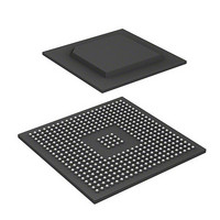
R8A77850ANBGV Renesas Electronics America, R8A77850ANBGV Datasheet - Page 224

R8A77850ANBGV
Manufacturer Part Number
R8A77850ANBGV
Description
IC SUPERH MPU ROMLESS 436-BGA
Manufacturer
Renesas Electronics America
Series
SuperH® SH7780r
Datasheet
1.R8A77850AADBGV.pdf
(1694 pages)
Specifications of R8A77850ANBGV
Core Processor
SH-4A
Core Size
32-Bit
Speed
600MHz
Connectivity
Audio Codec, MMC, Serial Sound, SCI, SIO, SPI, SSI
Peripherals
DMA, POR, WDT
Number Of I /o
108
Program Memory Type
ROMless
Ram Size
8K x 8
Voltage - Supply (vcc/vdd)
1 V ~ 1.2 V
Oscillator Type
External
Operating Temperature
-20°C ~ 75°C
Package / Case
436-BGA
Lead Free Status / RoHS Status
Lead free / RoHS Compliant
Eeprom Size
-
Program Memory Size
-
Data Converters
-
Available stocks
Company
Part Number
Manufacturer
Quantity
Price
Company:
Part Number:
R8A77850ANBGV
Manufacturer:
Renesas Electronics America
Quantity:
10 000
- Current page: 224 of 1694
- Download datasheet (9Mb)
7. Memory Management Unit (MMU)
7.7.2
The ITLB data array is allocated to addresses H'F300 0000 to H'F37F FFFF in the P4 area. A data
array access requires a 32-bit address field specification (when reading or writing) and a 32-bit
data field specification (when writing). Information for selecting the entry to be accessed is
specified in the address field, and PPN, V, SZ, PR, C, and SH to be written to the data array are
specified in the data field.
In the address field, bits [31:23] have the value H'F30 indicating ITLB data array and the entry is
specified by bits [9:8].
In the data field, bits [28:10] indicate PPN, bit [8] indicates V, bits [7] and [4] indicate SZ, bit [6]
indicates PR, bit [3] indicates C, and bit [1] indicates SH.
The following two kinds of operation can be used on ITLB data array:
1. ITLB data array read
2. ITLB data array write
Rev.1.00 Jan. 10, 2008 Page 192 of 1658
REJ09B0261-0100
PPN, V, SZ, PR, C, and SH are read into the data field from the ITLB entry corresponding to
the entry set in the address field.
PPN, V, SZ, PR, C, and SH specified in the data field are written to the ITLB entry
corresponding to the entry set in the address field.
Figure 7.19 Memory-Mapped ITLB Data Array (TLB Compatible Mode)
ITLB Data Array (TLB Compatible Mode)
Address field
Data field
SZ[1:0]:
31
31
1 1 1 1 0 0
PPN:
30 29 28
V:
E:
* :
Physical page number
Validity bit
Entry
Page size bits
Don't care
1 1
24
23
0
* * * * * * * * * * * *
PPN
PR:
SH:
C:
:
Protection key data
Cacheability bit
Share status bit
Reserved bits (write value should be 0,
and read value is undefined )
10 9 8 7
10 9 8 7
E
V
SZ1
* * * * * *
PR
6 5
SZ0
4 3
C
2 1
2 1 0
SH
0 0
0
Related parts for R8A77850ANBGV
Image
Part Number
Description
Manufacturer
Datasheet
Request
R

Part Number:
Description:
KIT STARTER FOR M16C/29
Manufacturer:
Renesas Electronics America
Datasheet:

Part Number:
Description:
KIT STARTER FOR R8C/2D
Manufacturer:
Renesas Electronics America
Datasheet:

Part Number:
Description:
R0K33062P STARTER KIT
Manufacturer:
Renesas Electronics America
Datasheet:

Part Number:
Description:
KIT STARTER FOR R8C/23 E8A
Manufacturer:
Renesas Electronics America
Datasheet:

Part Number:
Description:
KIT STARTER FOR R8C/25
Manufacturer:
Renesas Electronics America
Datasheet:

Part Number:
Description:
KIT STARTER H8S2456 SHARPE DSPLY
Manufacturer:
Renesas Electronics America
Datasheet:

Part Number:
Description:
KIT STARTER FOR R8C38C
Manufacturer:
Renesas Electronics America
Datasheet:

Part Number:
Description:
KIT STARTER FOR R8C35C
Manufacturer:
Renesas Electronics America
Datasheet:

Part Number:
Description:
KIT STARTER FOR R8CL3AC+LCD APPS
Manufacturer:
Renesas Electronics America
Datasheet:

Part Number:
Description:
KIT STARTER FOR RX610
Manufacturer:
Renesas Electronics America
Datasheet:

Part Number:
Description:
KIT STARTER FOR R32C/118
Manufacturer:
Renesas Electronics America
Datasheet:

Part Number:
Description:
KIT DEV RSK-R8C/26-29
Manufacturer:
Renesas Electronics America
Datasheet:

Part Number:
Description:
KIT STARTER FOR SH7124
Manufacturer:
Renesas Electronics America
Datasheet:

Part Number:
Description:
KIT STARTER FOR H8SX/1622
Manufacturer:
Renesas Electronics America
Datasheet:

Part Number:
Description:
KIT DEV FOR SH7203
Manufacturer:
Renesas Electronics America
Datasheet:


