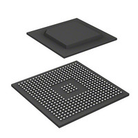
R8A77850ANBGV Renesas Electronics America, R8A77850ANBGV Datasheet - Page 459

R8A77850ANBGV
Manufacturer Part Number
R8A77850ANBGV
Description
IC SUPERH MPU ROMLESS 436-BGA
Manufacturer
Renesas Electronics America
Series
SuperH® SH7780r
Datasheet
1.R8A77850AADBGV.pdf
(1694 pages)
Specifications of R8A77850ANBGV
Core Processor
SH-4A
Core Size
32-Bit
Speed
600MHz
Connectivity
Audio Codec, MMC, Serial Sound, SCI, SIO, SPI, SSI
Peripherals
DMA, POR, WDT
Number Of I /o
108
Program Memory Type
ROMless
Ram Size
8K x 8
Voltage - Supply (vcc/vdd)
1 V ~ 1.2 V
Oscillator Type
External
Operating Temperature
-20°C ~ 75°C
Package / Case
436-BGA
Lead Free Status / RoHS Status
Lead free / RoHS Compliant
Eeprom Size
-
Program Memory Size
-
Data Converters
-
Available stocks
Company
Part Number
Manufacturer
Quantity
Price
Company:
Part Number:
R8A77850ANBGV
Manufacturer:
Renesas Electronics America
Quantity:
10 000
- Current page: 459 of 1694
- Download datasheet (9Mb)
11.5.6
When both the MODE 7 pin is set to 0 at a power-on reset by the PRESET pin, the MPX interface
is selected for area 0. The MPX interface is selected for areas 1 to 6 by the MPX bit in CS1BCR,
CS2BCR, and CS4BCR to CS6BCR. The MPX interface provides an address/data multiplex-type
bus protocol and facilitates connection with external memory controller chips using an
address/data multiplex-type 64- or 32-bit single bus. A bus cycle consists of an address phase and
a data phase. In the address phase, address information is output on D25 to D0, and the access size
is output on D63 to D61 for the 64-bit bus and on D31 to D29 for the 32-bit bus. The BS signal is
asserted for one cycle to indicate the address phase. The CSn signal is asserted at the rising edge in
Tm1 and is negated after the end of the last data transfer in the data phase. Therefore, a negation
cycle is not generated in the case of minimum pitch access. The FRAME signal is asserted at the
rising edge in Tm1 and negated at the start of the last data transfer cycle in the data phase.
Therefore, an external device for the MPX interface must internally store the address information
and access size output in the address phase and perform data input/output for the data phase. For
details, see section 11.5.1, Endian/Access Size and Data Alignment.
Values output to address pins A25 to A0 are not guaranteed.
In 32-byte transfer, a total of 32 bytes are transferred continuously according to the set bus width.
The first access is performed on the data for which an access request is issued, and the remaining
accesses are performed according to the set bus width. If the access size is larger than the bus
width, a burst access with continuing multiple data cycles occurs after one address output. The bus
is not released during this transfer.
Table 11.17 Relationship between D63/D31 to D61/D29 and Access Size in Address Phase
Legend:
X: Don't care
D63/D31
0
1
MPX Interface
D62/D30
0
1
X
D61/D29
0
1
0
1
X
Access Size
Byte
Word
Longword
Unused
32-byte burst
Rev.1.00 Jan. 10, 2008 Page 427 of 1658
11. Local Bus State Controller (LBSC)
REJ09B0261-0100
Related parts for R8A77850ANBGV
Image
Part Number
Description
Manufacturer
Datasheet
Request
R

Part Number:
Description:
KIT STARTER FOR M16C/29
Manufacturer:
Renesas Electronics America
Datasheet:

Part Number:
Description:
KIT STARTER FOR R8C/2D
Manufacturer:
Renesas Electronics America
Datasheet:

Part Number:
Description:
R0K33062P STARTER KIT
Manufacturer:
Renesas Electronics America
Datasheet:

Part Number:
Description:
KIT STARTER FOR R8C/23 E8A
Manufacturer:
Renesas Electronics America
Datasheet:

Part Number:
Description:
KIT STARTER FOR R8C/25
Manufacturer:
Renesas Electronics America
Datasheet:

Part Number:
Description:
KIT STARTER H8S2456 SHARPE DSPLY
Manufacturer:
Renesas Electronics America
Datasheet:

Part Number:
Description:
KIT STARTER FOR R8C38C
Manufacturer:
Renesas Electronics America
Datasheet:

Part Number:
Description:
KIT STARTER FOR R8C35C
Manufacturer:
Renesas Electronics America
Datasheet:

Part Number:
Description:
KIT STARTER FOR R8CL3AC+LCD APPS
Manufacturer:
Renesas Electronics America
Datasheet:

Part Number:
Description:
KIT STARTER FOR RX610
Manufacturer:
Renesas Electronics America
Datasheet:

Part Number:
Description:
KIT STARTER FOR R32C/118
Manufacturer:
Renesas Electronics America
Datasheet:

Part Number:
Description:
KIT DEV RSK-R8C/26-29
Manufacturer:
Renesas Electronics America
Datasheet:

Part Number:
Description:
KIT STARTER FOR SH7124
Manufacturer:
Renesas Electronics America
Datasheet:

Part Number:
Description:
KIT STARTER FOR H8SX/1622
Manufacturer:
Renesas Electronics America
Datasheet:

Part Number:
Description:
KIT DEV FOR SH7203
Manufacturer:
Renesas Electronics America
Datasheet:


