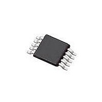
SI4010-C2-GT Silicon Laboratories Inc, SI4010-C2-GT Datasheet - Page 106

SI4010-C2-GT
Manufacturer Part Number
SI4010-C2-GT
Description
IC TX 27-960MHZ FSK 3.6V 10MSOP
Manufacturer
Silicon Laboratories Inc
Series
EZRadio®r
Type
Crystalless SoC RF Transmitterr
Datasheet
1.SI4010-C2-GT.pdf
(156 pages)
Specifications of SI4010-C2-GT
Package / Case
10-MSOP
Mfg Application Notes
SI4010 Calculator Spreadsheet AppNote
Frequency
27MHz ~ 960MHz
Applications
Garage Openers, RKE, Security Alarms
Modulation Or Protocol
FSK, OOK
Data Rate - Maximum
100 kBaud
Power - Output
10dBm
Current - Transmitting
19.8mA
Data Interface
PCB, Surface Mount
Antenna Connector
PCB, Surface Mount
Memory Size
4kB RAM
Features
8051 MCU Core, Crystal-less Operation
Voltage - Supply
1.8 V ~ 3.6 V
Operating Temperature
-40°C ~ 85°C
Operating Frequency
27 MHz to 960 MHz
Maximum Operating Temperature
+ 85 C
Mounting Style
SMD/SMT
Operating Supply Voltage
1.8 V to 3.6 V
Supply Current
14.2 mA
Lead Free Status / RoHS Status
Lead free / RoHS Compliant
Lead Free Status / RoHS Status
Lead free / RoHS Compliant, Lead free / RoHS Compliant
Other names
336-1997-5
Available stocks
Company
Part Number
Manufacturer
Quantity
Price
Part Number:
SI4010-C2-GT
Manufacturer:
SILICON LABS/èٹ¯ç§‘
Quantity:
20 000
Company:
Part Number:
SI4010-C2-GTR
Manufacturer:
ST
Quantity:
1 000
Part Number:
SI4010-C2-GTR
Manufacturer:
SILICON LABS/èٹ¯ç§‘
Quantity:
20 000
Si4010-C2
29. Reset Sources
Reset circuitry allows the controller to be easily placed in a predefined default condition. There is only one
external reset source for the device, which is power on reset. It gets invoked at two occasions:
1. Power is supplied to the device. This means connecting the power supply to disconnected device or
2. The device is waking up from a shutdown/standby mode. The power supply was connected before, but
On entry to the reset state, the following events occur:
All SFRs are reset to the predefined values noted in the SFR detailed descriptions. The contents of internal
data memory is lost since the power got cycled.
The Port I/O latches are reset to 0xFF (all logic ones) in open-drain mode.
On exit from the reset state, the program counter (PC) is reset, and the system clock defaults to the inter-
nal oscillator frequency of 24 MHz. Device starts its startup boot procedure. See other sections for descrip-
tion of the boot procedure. The user code starts being executed only after the boot procedure finishes. See
section 24. System Boot and NVM Programming for details.
29.1. Device Boot Outline
Since the device does not have flash memory to permanently hold user code, the device has to go through
a boot sequence in which the user code is copied from the one time programmable NVM memory to the
CODE/XDATA RAM. After that is done the user program execution starts at address 0x0000.
It takes about fixed 2 ms plus about 3.6 ms per 1 kB of user data to be copied from NVM to RAM. When
the user puts the device into shutdown mode this will be the estimated time for waking up the chip from
shutdown mode by applying any GPIO to ground and the execution of the first instruction of the user code
in CODE/XDATA RAM.
For debugging purposes the user will not program the NVM, but will use the RAM for code development. In
that case the device will go through much shorter startup routine, which would take less than 2 ms to con-
clude.
See “24. System Boot and NVM Programming” on page 69 for details.
29.2. External Reset
There is no external reset. There is no pin dedicated to the device reset. The Silicon Labs debug chain
using USB debug adapter or ToolStick has access to the proprietary reset control on chip to facilitate user
code debug and development. During the debugging sessions on unprogrammed part the content of the
CODE/XDATA RAM is preserved in between IDE environment invoked resets (Reset button inside IDE).
106
cycling the external power to the device.
the device was put into the shutdown/standby mode. The wake up event can happen because of two
reasons:
- One of the GPIOs is pulled low (e.g., a push button is pressed).
- The (previously enabled) sleep timer is expired.
CIP-51 halts program execution
Special Function Registers (SFR) are initialized to their defined reset values
XDATA registers (XREG) are initialized to their defined reset values
External Port pins are forced to a known state
Interrupts and timers are disabled
Rev. 1.0


