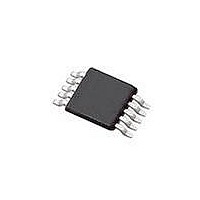
SI4010-C2-GT Silicon Laboratories Inc, SI4010-C2-GT Datasheet - Page 117

SI4010-C2-GT
Manufacturer Part Number
SI4010-C2-GT
Description
IC TX 27-960MHZ FSK 3.6V 10MSOP
Manufacturer
Silicon Laboratories Inc
Series
EZRadio®r
Type
Crystalless SoC RF Transmitterr
Datasheet
1.SI4010-C2-GT.pdf
(156 pages)
Specifications of SI4010-C2-GT
Package / Case
10-MSOP
Mfg Application Notes
SI4010 Calculator Spreadsheet AppNote
Frequency
27MHz ~ 960MHz
Applications
Garage Openers, RKE, Security Alarms
Modulation Or Protocol
FSK, OOK
Data Rate - Maximum
100 kBaud
Power - Output
10dBm
Current - Transmitting
19.8mA
Data Interface
PCB, Surface Mount
Antenna Connector
PCB, Surface Mount
Memory Size
4kB RAM
Features
8051 MCU Core, Crystal-less Operation
Voltage - Supply
1.8 V ~ 3.6 V
Operating Temperature
-40°C ~ 85°C
Operating Frequency
27 MHz to 960 MHz
Maximum Operating Temperature
+ 85 C
Mounting Style
SMD/SMT
Operating Supply Voltage
1.8 V to 3.6 V
Supply Current
14.2 mA
Lead Free Status / RoHS Status
Lead free / RoHS Compliant
Lead Free Status / RoHS Status
Lead free / RoHS Compliant, Lead free / RoHS Compliant
Other names
336-1997-5
Available stocks
Company
Part Number
Manufacturer
Quantity
Price
Part Number:
SI4010-C2-GT
Manufacturer:
SILICON LABS/èٹ¯ç§‘
Quantity:
20 000
Company:
Part Number:
SI4010-C2-GTR
Manufacturer:
ST
Quantity:
1 000
Part Number:
SI4010-C2-GTR
Manufacturer:
SILICON LABS/èٹ¯ç§‘
Quantity:
20 000
30.6. LED Driver on GPIO[5]
For application mode the GPIO[5] is shared with LED current driver. The LED current driver provides three
levels of LED current, 1mA maximum. The current levels are described in SFR Definition 30.6. User can
set the current intensity and then control the LED on and off by P0.5, port P0 bit 5, as a regular output.
There is no need to modify the P0CON.5 bit, since the GPIO[5] output driver is set to be open drain. When
the LED driver is on by setting the P0.5=1 then the pulldown output transistor is disabled. The GPIO[5] is
used as a regular open drain output during the C2 debugging sessions only.
During the C2 debug sessions the IDE will forcibly disable the LED driver so the LED drive will not interfere
with the debugging session. There will be an option on IDE to disable the “LED disable”, but it will have to
be used with caution.
When the user hits Disconnect button on the IDE then the IDE clears all breakpoint, removes the LED dis-
able, and runs the application from the point where it was halted. Then the application will control the LED.
The user then can hit the Connect button on the IDE to connect to the chip again. For the IDE to be able
to connect to the chip the LED must not be driven (not lit).
Figure 30.5. GPIO[5] LED Driver Block Diagram
PORT_CTRL
50k
VDD
2
Rev. 1.0
GPIO[5]/LED
Debug LED disable
P0
VDD
Si4010-C2
117


