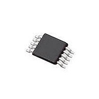
SI4010-C2-GT Silicon Laboratories Inc, SI4010-C2-GT Datasheet - Page 69

SI4010-C2-GT
Manufacturer Part Number
SI4010-C2-GT
Description
IC TX 27-960MHZ FSK 3.6V 10MSOP
Manufacturer
Silicon Laboratories Inc
Series
EZRadio®r
Type
Crystalless SoC RF Transmitterr
Datasheet
1.SI4010-C2-GT.pdf
(156 pages)
Specifications of SI4010-C2-GT
Package / Case
10-MSOP
Mfg Application Notes
SI4010 Calculator Spreadsheet AppNote
Frequency
27MHz ~ 960MHz
Applications
Garage Openers, RKE, Security Alarms
Modulation Or Protocol
FSK, OOK
Data Rate - Maximum
100 kBaud
Power - Output
10dBm
Current - Transmitting
19.8mA
Data Interface
PCB, Surface Mount
Antenna Connector
PCB, Surface Mount
Memory Size
4kB RAM
Features
8051 MCU Core, Crystal-less Operation
Voltage - Supply
1.8 V ~ 3.6 V
Operating Temperature
-40°C ~ 85°C
Operating Frequency
27 MHz to 960 MHz
Maximum Operating Temperature
+ 85 C
Mounting Style
SMD/SMT
Operating Supply Voltage
1.8 V to 3.6 V
Supply Current
14.2 mA
Lead Free Status / RoHS Status
Lead free / RoHS Compliant
Lead Free Status / RoHS Status
Lead free / RoHS Compliant, Lead free / RoHS Compliant
Other names
336-1997-5
Available stocks
Company
Part Number
Manufacturer
Quantity
Price
Part Number:
SI4010-C2-GT
Manufacturer:
SILICON LABS/èٹ¯ç§‘
Quantity:
20 000
Company:
Part Number:
SI4010-C2-GTR
Manufacturer:
ST
Quantity:
1 000
Part Number:
SI4010-C2-GTR
Manufacturer:
SILICON LABS/èٹ¯ç§‘
Quantity:
20 000
Si4010-C2
24. System Boot and NVM Programming
The device does not include a Flash memory for permanent code or data storage. Instead, the device con-
tains 4. 5kB of RAM, which can serve as a unified CODE and XDATA RAM memory. The device contains
8 kB of NVM (OTP) memory for user code and data storage. Small part of the NVM is reserved for Silicon
Labs factory use and is not available to a user. In general more than 7 kB of NVM will be available for user
application use.
24.1. Startup Overview
The code cannot be run directly from NVM, since it is not mapped directly to the CPU address space.
Instead, upon device reset, the device goes through a boot process during which the factory chip configu-
ration and the user application code and data is copied from NVM to the CODE/XDATA RAM. Only after
the boot process finishes the user code starts being executed from CODE/XDATA RAM address 0x0000.
Therefore upon reset the device does not execute the user code immediately, but only after the boot pro-
cess finishes. The time in between the device wakeup, either caused by cycling the power or waking up
from the shutdown mode by button press, depends on the size of the user code load.
In general the startup time is about 2ms of fixed time plus 3.6 ms per 1 kB of user application code. For
example, 4 kB application will incur
Tstartup = 2 ms + 3.6 ms x User_KB = 2 ms + 3.6 ms x 4 = 16.4 ms
startup time before the user application starts being executed.
For debugging purposes user will not program the NVM, but will use the RAM for code development. In
that case the device will only contain factory settings and go through much shorter startup routine, which
would take less than 2 ms to finish.
Rev. 1.0
69


