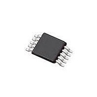
SI4010-C2-GT Silicon Laboratories Inc, SI4010-C2-GT Datasheet - Page 122

SI4010-C2-GT
Manufacturer Part Number
SI4010-C2-GT
Description
IC TX 27-960MHZ FSK 3.6V 10MSOP
Manufacturer
Silicon Laboratories Inc
Series
EZRadio®r
Type
Crystalless SoC RF Transmitterr
Datasheet
1.SI4010-C2-GT.pdf
(156 pages)
Specifications of SI4010-C2-GT
Package / Case
10-MSOP
Mfg Application Notes
SI4010 Calculator Spreadsheet AppNote
Frequency
27MHz ~ 960MHz
Applications
Garage Openers, RKE, Security Alarms
Modulation Or Protocol
FSK, OOK
Data Rate - Maximum
100 kBaud
Power - Output
10dBm
Current - Transmitting
19.8mA
Data Interface
PCB, Surface Mount
Antenna Connector
PCB, Surface Mount
Memory Size
4kB RAM
Features
8051 MCU Core, Crystal-less Operation
Voltage - Supply
1.8 V ~ 3.6 V
Operating Temperature
-40°C ~ 85°C
Operating Frequency
27 MHz to 960 MHz
Maximum Operating Temperature
+ 85 C
Mounting Style
SMD/SMT
Operating Supply Voltage
1.8 V to 3.6 V
Supply Current
14.2 mA
Lead Free Status / RoHS Status
Lead free / RoHS Compliant
Lead Free Status / RoHS Status
Lead free / RoHS Compliant, Lead free / RoHS Compliant
Other names
336-1997-5
Available stocks
Company
Part Number
Manufacturer
Quantity
Price
Part Number:
SI4010-C2-GT
Manufacturer:
SILICON LABS/èٹ¯ç§‘
Quantity:
20 000
Company:
Part Number:
SI4010-C2-GTR
Manufacturer:
ST
Quantity:
1 000
Part Number:
SI4010-C2-GTR
Manufacturer:
SILICON LABS/èٹ¯ç§‘
Quantity:
20 000
Si4010-C2
SFR Definition 30.7. PORT_SET
SFR Address = 0xB6
122
Name
Reset
5:4
1:0
Bit
Type
7
6
3
2
Bit
Reserved
CLKOUT
EDGE_
EDGE_
REFEN
PORT_
PORT_
CLKEN
PORT_
Name
INT1
INT0
EDGE_
[1:0]
INT1
R/W
7
0
Edge Control for INT1.
This bit controls whether single edge or both edges invoke the interrupt.
0: Single edge, polarity specified by NEG_INT1 in PORT_INTCFG.
1: Both edges, which means any edge, invoke INT1 interrupt.
Edge Control for INT0.
This bit controls whether single edge or both edges invoke the interrupt.
0: Single edge, polarity specified by NEG_INT0 in PORT_INTCFG.
1: Both edges, which means any edge, invoke INT0 interrupt.
Select which GPIO Pin is used as Clock Output Pin.
PORT_CLKOUT[0]: 1 .. clk output at GPIO[4], 0 .. normal/other GPIO[4] operation
PORT_CLKOUT[1]: 1 .. clk output at GPIO[6], 0 .. normal/other GPIO[6] operation
Both outputs can be used simultaneously. The actual clock waveform can be
enabled/disabled by port_clken bit, but the GPIO configuration is purely controlled by
PORT_CLKOUT.
Enable Output Clock, Which is Possibly Coming out on GPIO[4] and/or
GPIO[6].
This bit is just a clock enable/disable, it does not configure the GPIO for clock out-
puts. The port configuration must be done by port_clkout below. The generated clock
division is controlled by CLKOUT_SET register. If the clock is disabled by
PORT_CLKEN=0 the current period in progress will be finished and the output clock
will stop as logic 0.
Enable CLK_REF Reference Clock to come from GPIO[3].
The GPIO[3] pad is forced to be an input. There is not need to change p0 or p0con
register values, since port_refen has higher priority.
These bits must be left at 0.
EDGE_
INT0
R/W
6
0
PORT_CLKOUT[1:0]
R/W
5
0
R/W
Rev. 1.0
4
0
Function
PORT_
CLKEN
R/W
3
0
REFEN
PORT_
R/W
2
0
Reserved
R/W
1
0
Reserved
R/W
0
0


