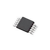
SI4010-C2-GT Silicon Laboratories Inc, SI4010-C2-GT Datasheet - Page 64

SI4010-C2-GT
Manufacturer Part Number
SI4010-C2-GT
Description
IC TX 27-960MHZ FSK 3.6V 10MSOP
Manufacturer
Silicon Laboratories Inc
Series
EZRadio®r
Type
Crystalless SoC RF Transmitterr
Datasheet
1.SI4010-C2-GT.pdf
(156 pages)
Specifications of SI4010-C2-GT
Package / Case
10-MSOP
Mfg Application Notes
SI4010 Calculator Spreadsheet AppNote
Frequency
27MHz ~ 960MHz
Applications
Garage Openers, RKE, Security Alarms
Modulation Or Protocol
FSK, OOK
Data Rate - Maximum
100 kBaud
Power - Output
10dBm
Current - Transmitting
19.8mA
Data Interface
PCB, Surface Mount
Antenna Connector
PCB, Surface Mount
Memory Size
4kB RAM
Features
8051 MCU Core, Crystal-less Operation
Voltage - Supply
1.8 V ~ 3.6 V
Operating Temperature
-40°C ~ 85°C
Operating Frequency
27 MHz to 960 MHz
Maximum Operating Temperature
+ 85 C
Mounting Style
SMD/SMT
Operating Supply Voltage
1.8 V to 3.6 V
Supply Current
14.2 mA
Lead Free Status / RoHS Status
Lead free / RoHS Compliant
Lead Free Status / RoHS Status
Lead free / RoHS Compliant, Lead free / RoHS Compliant
Other names
336-1997-5
Available stocks
Company
Part Number
Manufacturer
Quantity
Price
Part Number:
SI4010-C2-GT
Manufacturer:
SILICON LABS/èٹ¯ç§‘
Quantity:
20 000
Company:
Part Number:
SI4010-C2-GTR
Manufacturer:
ST
Quantity:
1 000
Part Number:
SI4010-C2-GTR
Manufacturer:
SILICON LABS/èٹ¯ç§‘
Quantity:
20 000
Si4010-C2
SFR Definition 22.6. PSW
SFR Address = 0xD0; Bit-Addressable
64
Name
Reset
4:3
Bit
Type
7
6
5
2
1
0
Bit
PARITY
RS[1:0]
Name
CY
AC
OV
F0
F1
R/W
CY
7
0
Carry Flag.
This bit is set when the last arithmetic operation resulted in a carry (addition) or a bor-
row (subtraction). It is cleared to logic 0 by all other arithmetic operations.
Auxiliary Carry Flag.
This bit is set when the last arithmetic operation resulted in a carry into (addition) or a
borrow from (subtraction) the high order nibble. It is cleared to logic 0 by all other arith-
metic operations.
User Flag 0.
This is a bit-addressable, general purpose flag for use under software control.
Register Bank Select.
These bits select which register bank is used during register accesses.
00: Bank 0, Addresses 0x00-0x07
01: Bank 1, Addresses 0x08-0x0F
10: Bank 2, Addresses 0x10-0x17
11: Bank 3, Addresses 0x18-0x1F
Overflow Flag.
This bit is set to 1 under the following circumstances:
The OV bit is cleared to 0 by the ADD, ADDC, SUBB, MUL, and DIV instructions in all
other cases.
User Flag 1.
This is a bit-addressable, general purpose flag for use under software control.
Parity Flag.
This bit is set to logic 1 if the sum of the eight bits in the accumulator is odd and cleared
if the sum is even.
l
l
l
An ADD, ADDC, or SUBB instruction causes a sign-change overflow.
A MUL instruction results in an overflow (result is greater than 255).
A DIV instruction causes a divide-by-zero condition.
R/W
AC
6
0
R/W
F0
5
0
Rev. 1.0
4
0
RS[1:0]
R/W
Function
3
0
R/W
OV
2
0
R/W
F1
1
0
PARITY
R
0
0


