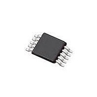
SI4010-C2-GT Silicon Laboratories Inc, SI4010-C2-GT Datasheet - Page 99

SI4010-C2-GT
Manufacturer Part Number
SI4010-C2-GT
Description
IC TX 27-960MHZ FSK 3.6V 10MSOP
Manufacturer
Silicon Laboratories Inc
Series
EZRadio®r
Type
Crystalless SoC RF Transmitterr
Datasheet
1.SI4010-C2-GT.pdf
(156 pages)
Specifications of SI4010-C2-GT
Package / Case
10-MSOP
Mfg Application Notes
SI4010 Calculator Spreadsheet AppNote
Frequency
27MHz ~ 960MHz
Applications
Garage Openers, RKE, Security Alarms
Modulation Or Protocol
FSK, OOK
Data Rate - Maximum
100 kBaud
Power - Output
10dBm
Current - Transmitting
19.8mA
Data Interface
PCB, Surface Mount
Antenna Connector
PCB, Surface Mount
Memory Size
4kB RAM
Features
8051 MCU Core, Crystal-less Operation
Voltage - Supply
1.8 V ~ 3.6 V
Operating Temperature
-40°C ~ 85°C
Operating Frequency
27 MHz to 960 MHz
Maximum Operating Temperature
+ 85 C
Mounting Style
SMD/SMT
Operating Supply Voltage
1.8 V to 3.6 V
Supply Current
14.2 mA
Lead Free Status / RoHS Status
Lead free / RoHS Compliant
Lead Free Status / RoHS Status
Lead free / RoHS Compliant, Lead free / RoHS Compliant
Other names
336-1997-5
Available stocks
Company
Part Number
Manufacturer
Quantity
Price
Part Number:
SI4010-C2-GT
Manufacturer:
SILICON LABS/èٹ¯ç§‘
Quantity:
20 000
Company:
Part Number:
SI4010-C2-GTR
Manufacturer:
ST
Quantity:
1 000
Part Number:
SI4010-C2-GTR
Manufacturer:
SILICON LABS/èٹ¯ç§‘
Quantity:
20 000
Si4010-C2
26.5. External Interrupts
The INT0 and INT1 external interrupt sources are configurable as active high or low. They are edge sensi-
tive only, not level sensitive. These are not the same INT0 and INT1 as found on original 8051 architecture.
Each of the INT0 and INT1 can invoke interrupt on the rising edge, falling edge, or both edges of the
selected GPIO pins associated with the INT0 and INT1, respectively.
The single edge or double edge feature is controlled by the EDGE_INT0 and EDGE_INT1 bits in the
PORT_SET register. The edge polarity is defined in the PORT_INTCFG register.
INT0 and INT1 are assigned to Port pins as defined in the PORT_INTCFG register. Note that the corre-
sponding pending flag for INT0 or INT1 is not automatically cleared by the hardware when the CPU vec-
tors to the ISR. This is a departure from the original 8051 architecture where if external interrupts were
configured to be edge sensitive the corresponding interrupt flag was cleared by hardware upon the exit
from the ISR routine.
The detection of the edges of INT0 and INT1 sources is done by sampling the associated port inputs by the
internal system clock. Therefore, the edge detector will miss pulses shorter than 2 periods of the internal
system clock periods. Note that the internal system clock frequency is programmable and can be as low as
24 MHz/128. It is up to the user to recognize possible external interrupt delays associated with sampling of
the INT0 and INT1 by the system clock at the current, user selected, clock frequency.
The INT1 and INT0 internal signals are also used as capture event signals for timer 3 and 2, respectively,
if they are running in capture mode.
Rev. 1.0
99


