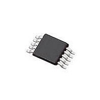
SI4010-C2-GT Silicon Laboratories Inc, SI4010-C2-GT Datasheet - Page 79

SI4010-C2-GT
Manufacturer Part Number
SI4010-C2-GT
Description
IC TX 27-960MHZ FSK 3.6V 10MSOP
Manufacturer
Silicon Laboratories Inc
Series
EZRadio®r
Type
Crystalless SoC RF Transmitterr
Datasheet
1.SI4010-C2-GT.pdf
(156 pages)
Specifications of SI4010-C2-GT
Package / Case
10-MSOP
Mfg Application Notes
SI4010 Calculator Spreadsheet AppNote
Frequency
27MHz ~ 960MHz
Applications
Garage Openers, RKE, Security Alarms
Modulation Or Protocol
FSK, OOK
Data Rate - Maximum
100 kBaud
Power - Output
10dBm
Current - Transmitting
19.8mA
Data Interface
PCB, Surface Mount
Antenna Connector
PCB, Surface Mount
Memory Size
4kB RAM
Features
8051 MCU Core, Crystal-less Operation
Voltage - Supply
1.8 V ~ 3.6 V
Operating Temperature
-40°C ~ 85°C
Operating Frequency
27 MHz to 960 MHz
Maximum Operating Temperature
+ 85 C
Mounting Style
SMD/SMT
Operating Supply Voltage
1.8 V to 3.6 V
Supply Current
14.2 mA
Lead Free Status / RoHS Status
Lead free / RoHS Compliant
Lead Free Status / RoHS Status
Lead free / RoHS Compliant, Lead free / RoHS Compliant
Other names
336-1997-5
Available stocks
Company
Part Number
Manufacturer
Quantity
Price
Part Number:
SI4010-C2-GT
Manufacturer:
SILICON LABS/èٹ¯ç§‘
Quantity:
20 000
Company:
Part Number:
SI4010-C2-GTR
Manufacturer:
ST
Quantity:
1 000
Part Number:
SI4010-C2-GTR
Manufacturer:
SILICON LABS/èٹ¯ç§‘
Quantity:
20 000
24.9. Boot Routine Destination Address Space
The boot process reads the formatted data from NVM and writes it to the desired destination. The format
supports different address regions based on the destination (write) address. The destination address is
part of the NVM content data frame format.
The address space of the NVM image destinations depend on the program level of the chip and is shown
in Figure 24.3:
It is up to the user to generate IntelHEX files to be passed to the NVM programmer. The NVM programmer
will ensure that the NVM gets programmed with a proper data structures such that the data values pro-
vided in the IntelHEX files will appear at the RAM and IRAM addresses specified in the IntelHEX input file
after the boot is done.
0x0000 .. 0x11FF .. CODE/XDATA RAM. The end of the RAM is reserved for the boot control data.
0x7000 .. 0x70FF .. virtually mapped 256 byte of IRAM for DATA/IDATA indirect access. Whenever the
destination address in the NVM image is in this region the data destination is going to be DATA/IDATA
IRAM space. However, only region 0x7020 .. 0x70EF is writable. That means that the first 32 and last
16 bytes of the IRAM are not writable by a boot process. Note that the mapping is for indirect internal
IRAM access (DATA/IDATA), so SFR registers cannot be initialized by this process.
Figure 24.3. Boot Routine Destination CPU Address Space for Copy from NVM
Boot routine view of the CPU memory space for writing
User data from the NVM to the RAM/register spaces
0xFFFF
0x11FF
0x0000
0x4000
0x7000
0x8000
Rev. 1.0
IRAM 256B
RAM 4.5K
Si4010-C2
79


