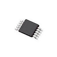
SI4010-C2-GT Silicon Laboratories Inc, SI4010-C2-GT Datasheet - Page 25

SI4010-C2-GT
Manufacturer Part Number
SI4010-C2-GT
Description
IC TX 27-960MHZ FSK 3.6V 10MSOP
Manufacturer
Silicon Laboratories Inc
Series
EZRadio®r
Type
Crystalless SoC RF Transmitterr
Datasheet
1.SI4010-C2-GT.pdf
(156 pages)
Specifications of SI4010-C2-GT
Package / Case
10-MSOP
Mfg Application Notes
SI4010 Calculator Spreadsheet AppNote
Frequency
27MHz ~ 960MHz
Applications
Garage Openers, RKE, Security Alarms
Modulation Or Protocol
FSK, OOK
Data Rate - Maximum
100 kBaud
Power - Output
10dBm
Current - Transmitting
19.8mA
Data Interface
PCB, Surface Mount
Antenna Connector
PCB, Surface Mount
Memory Size
4kB RAM
Features
8051 MCU Core, Crystal-less Operation
Voltage - Supply
1.8 V ~ 3.6 V
Operating Temperature
-40°C ~ 85°C
Operating Frequency
27 MHz to 960 MHz
Maximum Operating Temperature
+ 85 C
Mounting Style
SMD/SMT
Operating Supply Voltage
1.8 V to 3.6 V
Supply Current
14.2 mA
Lead Free Status / RoHS Status
Lead free / RoHS Compliant
Lead Free Status / RoHS Status
Lead free / RoHS Compliant, Lead free / RoHS Compliant
Other names
336-1997-5
Available stocks
Company
Part Number
Manufacturer
Quantity
Price
Part Number:
SI4010-C2-GT
Manufacturer:
SILICON LABS/èٹ¯ç§‘
Quantity:
20 000
Company:
Part Number:
SI4010-C2-GTR
Manufacturer:
ST
Quantity:
1 000
Part Number:
SI4010-C2-GTR
Manufacturer:
SILICON LABS/èٹ¯ç§‘
Quantity:
20 000
Notes:
General
Solder Mask Design
Stencil Design
Card Assembly
1. All dimensions shown are in millimeters (mm) unless otherwise noted.
2. Dimensioning and Tolerancing per ASME Y14.5M-1994.
3. This Land Pattern Design is based on the IPC-7351 guidelines.
4. All dimensions shown are at Maximum Material Condition (MMC).
1. All metal pads are to be non-solder mask defined (NSMD). Clearance
1. A stainless steel, laser-cut and electro-polished stencil with
2. The stencil thickness should be 0.125mm (5 mils).
3. The ratio of stencil aperture to land pad size should be 1:1.
1. A No-Clean, Type-3 solder paste is recommended.
2. The recommended card reflow profile is per the JEDEC/IPC J-STD-
Dimension
Least Material Condition (LMC) is calculated based on a Fabrication
Allowance of 0.05mm.
between the solder mask and the metal pad is to be 60 m minimum, all
the way around the pad.
trapezoidal walls should be used to assure good solder paste release.
020 specification for Small Body Components.
G1
C1
X1
Y1
Z1
E
Table 8.1. 10-Pin MSOP Dimensions
Rev. 1.0
3.00
MIN
—
—
4.40 REF
0.50 BSC
1.40 REF
MAX
0.30
5.80
—
Si4010-C2
25


