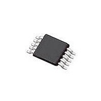
SI4010-C2-GT Silicon Laboratories Inc, SI4010-C2-GT Datasheet - Page 67

SI4010-C2-GT
Manufacturer Part Number
SI4010-C2-GT
Description
IC TX 27-960MHZ FSK 3.6V 10MSOP
Manufacturer
Silicon Laboratories Inc
Series
EZRadio®r
Type
Crystalless SoC RF Transmitterr
Datasheet
1.SI4010-C2-GT.pdf
(156 pages)
Specifications of SI4010-C2-GT
Package / Case
10-MSOP
Mfg Application Notes
SI4010 Calculator Spreadsheet AppNote
Frequency
27MHz ~ 960MHz
Applications
Garage Openers, RKE, Security Alarms
Modulation Or Protocol
FSK, OOK
Data Rate - Maximum
100 kBaud
Power - Output
10dBm
Current - Transmitting
19.8mA
Data Interface
PCB, Surface Mount
Antenna Connector
PCB, Surface Mount
Memory Size
4kB RAM
Features
8051 MCU Core, Crystal-less Operation
Voltage - Supply
1.8 V ~ 3.6 V
Operating Temperature
-40°C ~ 85°C
Operating Frequency
27 MHz to 960 MHz
Maximum Operating Temperature
+ 85 C
Mounting Style
SMD/SMT
Operating Supply Voltage
1.8 V to 3.6 V
Supply Current
14.2 mA
Lead Free Status / RoHS Status
Lead free / RoHS Compliant
Lead Free Status / RoHS Status
Lead free / RoHS Compliant, Lead free / RoHS Compliant
Other names
336-1997-5
Available stocks
Company
Part Number
Manufacturer
Quantity
Price
Part Number:
SI4010-C2-GT
Manufacturer:
SILICON LABS/èٹ¯ç§‘
Quantity:
20 000
Company:
Part Number:
SI4010-C2-GTR
Manufacturer:
ST
Quantity:
1 000
Part Number:
SI4010-C2-GTR
Manufacturer:
SILICON LABS/èٹ¯ç§‘
Quantity:
20 000
Si4010-C2
23.5. Bit Addressable Locations
In addition to direct access to data memory organized as bytes, the sixteen data memory locations at 0x20
through 0x2F are also accessible as 128 individually addressable bits. Each bit has a bit address from
0x00 to 0x7F. Bit 0 of the byte at 0x20 has bit address 0x00 while bit 7 of the byte at 0x20 has bit address
0x07. Bit 7 of the byte at 0x2F has bit address 0x7F. A bit access is distinguished from a full byte access by
the type of instruction used (bit source or destination operands as opposed to a byte source or destina-
tion).
The MCS-51™ assembly language allows an alternate notation for bit addressing of the form XX.B where
XX is the byte address and B is the bit position within the byte.
For example, the instruction:
MOV C, 22.3h
moves the Boolean value at 0x13 (bit 3 of the byte at location 0x22) into the Carry flag.
23.6. Stack
A programmer's stack can be located anywhere in the 256 byte data memory. The stack area is designated
using the Stack Pointer (SP, address 0x81) SFR. The SP will point to the last location used. The next value
pushed on the stack is placed at SP+1 and then SP is incremented. A reset initializes the stack pointer to
location 0x07; therefore, the first value pushed on the stack is placed at location 0x08, which is also the
first register (R0) of register bank 1. Thus, if more than one register bank is to be used, the SP should be
initialized to a location in the data memory not being used for data storage. The stack depth can extend up
to 256 bytes.
23.7. Special Function Registers (SFR)
The direct-access data memory locations from 0x80 to 0xFF constitute the special function registers
(SFRs). The SFRs provide control and data exchange with the CIP-51's resources and peripherals. The
CIP-51 duplicates the SFRs found in a typical 8051 implementation as well as implementing additional
SFRs used to configure and access the sub-systems unique to the MCU. This allows the addition of new
functionality while retaining compatibility with the MCS-51™ instruction set. Table 25.1 lists the SFRs
implemented in the device.
The SFR registers are accessed whenever the direct addressing mode is used to access memory loca-
tions from 0x80 to 0xFF. SFRs with addresses ending in 0x0 or 0x8 (e.g. P0, P1, IE, etc.) are bit-address-
able as well as byte-addressable. All other SFRs are byte-addressable only. Unoccupied addresses in the
SFR space are reserved for future use. Accessing these areas will have an indeterminate effect and
should be avoided. Refer to the corresponding pages of the data sheet for a detailed description of each
register.
23.8. Registers Mapped to XDATA Address Space (XREG)
Given the extensive requirement for the numerous hardware registers some of the registers are mapped to
the XDATA space as shown in Figure 23.1. Those registers are accessible only by MOVX instructions and
are viewed from the CPU as a regular external XDATA memory. Registers which are more than single byte
wide are organized in big endian fashion (most significant byte on the lowest address) to comply with the
Keil development toolchain. They can be declared as regular variables in higher level languages, like C.
Map of user accessible XREG registers is in Table 25.3.
23.9. NVM (OTP) Memory
NVM memory is only accessible indirectly through Silicon Labs provided API functions for NVM access ini-
tialization and read of formatted blocks of data generated by the NVM programmer. Programming of the
NVM can be only done by Silicon Labs provided tools. It is not possible to program the NVM by writing to
registers. See “System Boot and NVM Programming” on page 69 for details.
Rev. 1.0
67


