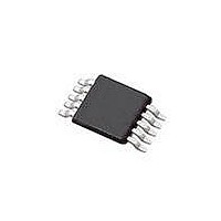
SI4010-C2-GT Silicon Laboratories Inc, SI4010-C2-GT Datasheet - Page 72

SI4010-C2-GT
Manufacturer Part Number
SI4010-C2-GT
Description
IC TX 27-960MHZ FSK 3.6V 10MSOP
Manufacturer
Silicon Laboratories Inc
Series
EZRadio®r
Type
Crystalless SoC RF Transmitterr
Datasheet
1.SI4010-C2-GT.pdf
(156 pages)
Specifications of SI4010-C2-GT
Package / Case
10-MSOP
Mfg Application Notes
SI4010 Calculator Spreadsheet AppNote
Frequency
27MHz ~ 960MHz
Applications
Garage Openers, RKE, Security Alarms
Modulation Or Protocol
FSK, OOK
Data Rate - Maximum
100 kBaud
Power - Output
10dBm
Current - Transmitting
19.8mA
Data Interface
PCB, Surface Mount
Antenna Connector
PCB, Surface Mount
Memory Size
4kB RAM
Features
8051 MCU Core, Crystal-less Operation
Voltage - Supply
1.8 V ~ 3.6 V
Operating Temperature
-40°C ~ 85°C
Operating Frequency
27 MHz to 960 MHz
Maximum Operating Temperature
+ 85 C
Mounting Style
SMD/SMT
Operating Supply Voltage
1.8 V to 3.6 V
Supply Current
14.2 mA
Lead Free Status / RoHS Status
Lead free / RoHS Compliant
Lead Free Status / RoHS Status
Lead free / RoHS Compliant, Lead free / RoHS Compliant
Other names
336-1997-5
Available stocks
Company
Part Number
Manufacturer
Quantity
Price
Part Number:
SI4010-C2-GT
Manufacturer:
SILICON LABS/èٹ¯ç§‘
Quantity:
20 000
Company:
Part Number:
SI4010-C2-GTR
Manufacturer:
ST
Quantity:
1 000
Part Number:
SI4010-C2-GTR
Manufacturer:
SILICON LABS/èٹ¯ç§‘
Quantity:
20 000
Si4010-C2
24.5. Device Boot Process
The boot process works in the following sequence:
1. Boot is invoked by cycling power to the internals of the chip (which includes power cycle to the whole
2. The device will read the Factory part of the NVM to determine the device configuration and load the
3. If the program level is Factory then the boot process will stop and will not execute any code. It will wait
4. If the program level is User then the same procedure is followed as for the Factory device. After that
72
chip), waking up by button press, by the sleep timer, or by pressing a Reset button in the IDE
development platform.
configuration values to appropriate registers and CODE/XDATA memory locations. Part of this process
is setting the boot variable block at the end of the CODE/XDATA memory.
in an infinite loop for the debugging chain to load a user application to CODE/XDATA RAM and to allow
that code execution from the IDE. More specifically, the boot hardware waits for the CODE_RUN_POR
or CODE_RUN_SYS bits to be set in the BOOT_FLAGS register. When using debugging chain and
IDE, this is taken care of automatically by the IDE and there is no user intervention required.
the boot procedure automatically (see Note 1.) continues to load User region from NVM to
CODE/XDATA RAM and IRAM. After it finishes the device does not execute any code (see Note 2.) and
goes to the same waiting infinite loop as described in item 3. for Factory device.
The user can modify the boot behavior of the User part by controlling the following two bits:
wBoot_NvmUserBeg
Note 1. BOOT_TRIM_POR bit in BOOT_FLAGS .. Register cleared on power on reset. If this bit is
Note 2. USER_CONT bit in PROT3_CTRL in NVM .. Bit in the NVM protection register. Once set it
factory setup
1, the boot loader will not load the User load but enables C2 and goes to the boot_flags
waiting loop. The part will behave as a Factory part. This bit has higher priority than the one
below. Convenient for debugging until the power is cycled.
Set by the
0xFFC0
0xFFFF
0xE000
NVM 8KB
Optional gap
(App Use)
Figure 24.1. NVM Address Map
User App
Reserved
Factory
Optional
64 bytes
(Boot)
Setup
User
Rev. 1.0
First unread NVM byte address .. User/Run part
wBoot_NvmCopyAddr


