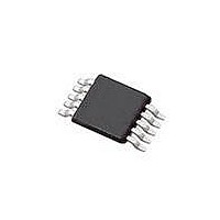
SI4010-C2-GT Silicon Laboratories Inc, SI4010-C2-GT Datasheet - Page 125

SI4010-C2-GT
Manufacturer Part Number
SI4010-C2-GT
Description
IC TX 27-960MHZ FSK 3.6V 10MSOP
Manufacturer
Silicon Laboratories Inc
Series
EZRadio®r
Type
Crystalless SoC RF Transmitterr
Datasheet
1.SI4010-C2-GT.pdf
(156 pages)
Specifications of SI4010-C2-GT
Package / Case
10-MSOP
Mfg Application Notes
SI4010 Calculator Spreadsheet AppNote
Frequency
27MHz ~ 960MHz
Applications
Garage Openers, RKE, Security Alarms
Modulation Or Protocol
FSK, OOK
Data Rate - Maximum
100 kBaud
Power - Output
10dBm
Current - Transmitting
19.8mA
Data Interface
PCB, Surface Mount
Antenna Connector
PCB, Surface Mount
Memory Size
4kB RAM
Features
8051 MCU Core, Crystal-less Operation
Voltage - Supply
1.8 V ~ 3.6 V
Operating Temperature
-40°C ~ 85°C
Operating Frequency
27 MHz to 960 MHz
Maximum Operating Temperature
+ 85 C
Mounting Style
SMD/SMT
Operating Supply Voltage
1.8 V to 3.6 V
Supply Current
14.2 mA
Lead Free Status / RoHS Status
Lead free / RoHS Compliant
Lead Free Status / RoHS Status
Lead free / RoHS Compliant, Lead free / RoHS Compliant
Other names
336-1997-5
Available stocks
Company
Part Number
Manufacturer
Quantity
Price
Part Number:
SI4010-C2-GT
Manufacturer:
SILICON LABS/èٹ¯ç§‘
Quantity:
20 000
Company:
Part Number:
SI4010-C2-GTR
Manufacturer:
ST
Quantity:
1 000
Part Number:
SI4010-C2-GTR
Manufacturer:
SILICON LABS/èٹ¯ç§‘
Quantity:
20 000
Bit
4:0
5
CLKOUT_
CLKOUT_
DIV[4:0]
Name
SYM
CLKOUT Symmetry.
If this bit set to 1 then the output clock duty cycle is very close to 1:1 irrespective of
the division factor. However, the generated clock waveform is a combination of
outputs of two flops and therefore might jitter more. If this bit is 0 then for odd division
factor there is a single 24 MHz period difference in between halves of the generation
output clock.
This bit must be set before customer clock is enabled to the port output by setting
PORT_SET.PORT_CLKEN=1.
CLKOUT Division Factor.
Division factor of the 24 MHz oscillator clock for generation of the output customer
clock. The enable of the clock is controlled by the PORT_CLKEN and
PORT_CLKOUT bits in PORT_SET register. The division factors 0 and 1 pass the
24 MHz internal cheap oscillator output as output clocks. Value bigger than 1 is the
actual division factor of the 24 MHz.
If CLKOUT_SYM=0 (recommended), the generated clock is an output of a flop. For
odd division ratios the first part of the period in logic 0 is one 24 MHz clock cycle
shorter than the second high half part of the period of generated clock, assuming
CLKOUT_INV=0.
If the clock is disabled by PORT_CLKEN=0 the current period in progress will be
finished. To monitor when the output gets idle monitor the CLKOUT_CLR bit of this
register.
The CLKOUT_DIV bit can be changed any time. The new setting will take effect only
after the current period finishes. For the new setting to take effect immediately see
CLKOUT_CLR.
Rev. 1.0
Function
Si4010-C2
125


