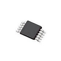
SI4010-C2-GT Silicon Laboratories Inc, SI4010-C2-GT Datasheet - Page 151

SI4010-C2-GT
Manufacturer Part Number
SI4010-C2-GT
Description
IC TX 27-960MHZ FSK 3.6V 10MSOP
Manufacturer
Silicon Laboratories Inc
Series
EZRadio®r
Type
Crystalless SoC RF Transmitterr
Datasheet
1.SI4010-C2-GT.pdf
(156 pages)
Specifications of SI4010-C2-GT
Package / Case
10-MSOP
Mfg Application Notes
SI4010 Calculator Spreadsheet AppNote
Frequency
27MHz ~ 960MHz
Applications
Garage Openers, RKE, Security Alarms
Modulation Or Protocol
FSK, OOK
Data Rate - Maximum
100 kBaud
Power - Output
10dBm
Current - Transmitting
19.8mA
Data Interface
PCB, Surface Mount
Antenna Connector
PCB, Surface Mount
Memory Size
4kB RAM
Features
8051 MCU Core, Crystal-less Operation
Voltage - Supply
1.8 V ~ 3.6 V
Operating Temperature
-40°C ~ 85°C
Operating Frequency
27 MHz to 960 MHz
Maximum Operating Temperature
+ 85 C
Mounting Style
SMD/SMT
Operating Supply Voltage
1.8 V to 3.6 V
Supply Current
14.2 mA
Lead Free Status / RoHS Status
Lead free / RoHS Compliant
Lead Free Status / RoHS Status
Lead free / RoHS Compliant, Lead free / RoHS Compliant
Other names
336-1997-5
Available stocks
Company
Part Number
Manufacturer
Quantity
Price
Part Number:
SI4010-C2-GT
Manufacturer:
SILICON LABS/èٹ¯ç§‘
Quantity:
20 000
Company:
Part Number:
SI4010-C2-GTR
Manufacturer:
ST
Quantity:
1 000
Part Number:
SI4010-C2-GTR
Manufacturer:
SILICON LABS/èٹ¯ç§‘
Quantity:
20 000
36. IDE Development Environment and Debugging Chain
The development platform will be provided by Silicon Labs. The debugging chain consists of an evaluation
board or an evaluation keyfob, USB debug adapter or a USB based ToolStick, and the Silicon Labs IDE
development environment.
The debugging chain is using the C2 two wire interface to provide an on-chip debugging capability. The
environment can load the standard OMF-51 object and symbol file only, not any proprietary extensions of
that format as used by some tool manufacturers. For example, on Keil platform it means that the BL51
linker must be used. The IDE will not load outputs generated by the Keil LX51 linker. On Raisonance plat-
form the output is the OMF-51 compliant and the file extension is AOF.
The IDE debugging environment has means to reset the chip without cycling the power. By pressing the
Reset inside of the IDE the digital part of the device is reset and device startup boot sequence is invoked.
All registers are reset to their initial states and all of the Factory values are refreshed in RAM and regis-
ters. If the part is a Factory part, the previously loaded CODE/XDATA RAM content is not disturbed. If the
part is a User part then the User data region is loaded as well, overwriting the content of the CODE/XDATA
RAM.
Using IDE is the only way to reset the chip without cycling the power to it or shutting it down and waking it
up.
36.1. Functionality Limitations While Using IDE Development Environment
Even though using the Silicon Labs IDE development environment preserves almost all of the chip func-
tionality, there are some limitations the user should be aware of. Given that the code is running from RAM
and that the C2CLK shares the pin with LED output current driver (GPIO[5]), they are two functionality lim-
itations for code development while using IDE:
1. The user cannot put a Factory or User chip into the shutdown mode and then wake it up by pressing a
2. The LED driver cannot be used when the device is connected to the debug adapters (USB debug
3. Once the part is finalized, programmed as Run part, no further debugging is possible.
button (pulling any of the GPIO to ground). When the chip is in shutdown mode, the power to all digital
is lost and therefore the RAM content with the user code will get erased.
adapter or a ToolStick).
Rev. 1.0
Si4010-C2
151


