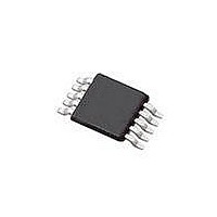
SI4010-C2-GT Silicon Laboratories Inc, SI4010-C2-GT Datasheet - Page 36

SI4010-C2-GT
Manufacturer Part Number
SI4010-C2-GT
Description
IC TX 27-960MHZ FSK 3.6V 10MSOP
Manufacturer
Silicon Laboratories Inc
Series
EZRadio®r
Type
Crystalless SoC RF Transmitterr
Datasheet
1.SI4010-C2-GT.pdf
(156 pages)
Specifications of SI4010-C2-GT
Package / Case
10-MSOP
Mfg Application Notes
SI4010 Calculator Spreadsheet AppNote
Frequency
27MHz ~ 960MHz
Applications
Garage Openers, RKE, Security Alarms
Modulation Or Protocol
FSK, OOK
Data Rate - Maximum
100 kBaud
Power - Output
10dBm
Current - Transmitting
19.8mA
Data Interface
PCB, Surface Mount
Antenna Connector
PCB, Surface Mount
Memory Size
4kB RAM
Features
8051 MCU Core, Crystal-less Operation
Voltage - Supply
1.8 V ~ 3.6 V
Operating Temperature
-40°C ~ 85°C
Operating Frequency
27 MHz to 960 MHz
Maximum Operating Temperature
+ 85 C
Mounting Style
SMD/SMT
Operating Supply Voltage
1.8 V to 3.6 V
Supply Current
14.2 mA
Lead Free Status / RoHS Status
Lead free / RoHS Compliant
Lead Free Status / RoHS Status
Lead free / RoHS Compliant, Lead free / RoHS Compliant
Other names
336-1997-5
Available stocks
Company
Part Number
Manufacturer
Quantity
Price
Part Number:
SI4010-C2-GT
Manufacturer:
SILICON LABS/èٹ¯ç§‘
Quantity:
20 000
Company:
Part Number:
SI4010-C2-GTR
Manufacturer:
ST
Quantity:
1 000
Part Number:
SI4010-C2-GTR
Manufacturer:
SILICON LABS/èٹ¯ç§‘
Quantity:
20 000
Si4010-C2
12. Power Amplifier
The CMOS power amplifier (PA) is a differential open drain amplifier capable of delivering +10 dBm of out-
put power. Maximum power can be transferred to an inductive antenna load when the antenna and output
driver of the PA are at resonance and the real component of the combined load is equal to the optimum
load resistance of V
current of the PA. This optimum load resistance is the parallel combination of the PA output resistance and
the differential antenna resistance. At higher resistances the PA is voltage limited and at lower resistances
the PA is current limited. The PA tail current is programmable from 810 µA up to 7.67 mA (SFR register
PA_LVL) in 0.25 dB steps and there is a boost current bit (XREG PA_TRIM.PA_MAX_DRV) that multiplies
the tail current by 1.5 times allowing it to go up to 11.5mA. The maximum differential peak-to-peak voltage
is 3.5 V when the supply is 2.2 to 3.6 V and drops linearly down to 3.0 V when the supply is at 1.8 V
The calculator spreadsheet tool computes the required antenna impedance and API settings to achieve
the user desired output power. Proper layout and matching techniques are all necessary to ensure optimal
performance. Figure 9.1 shows a typical application schematic of the Si4010 for a differential loop
antenna. Application note "AN369: Antenna Interface for the Si401x Transmitters" provides detailed infor-
mation about designing the antenna interface for the Si401X transmitters. With proper filtering and layout
techniques, the Si4010 can conform to US FCC part 15.231 and European EN 300 220 regulations. Edge
rate control is also included for OOK mode to reduce harmonics that may otherwise violate government
regulations. Edge shaping is accomplished by gradually turning on and off the driver transistors of the PA.
The edge shaping parameters are controlled by the ODS block and is automatically determined by the cal-
culator spread sheet based on the desired data rate and encoding method. Users must comply with local
radio frequency transmission regulations.
Off-chip capacitor tolerances, loop antenna manufacturing tolerances, and environmental variations can
lead to impedance mismatch at the PA output causing reduced radiated power level. The Si4010 includes
an automatic antenna tuning circuit to reduce the mismatch by adjusting the on-chip variable capacitor to
resonate with the inductance of the antenna. The PA output has 2.4 to 12.5 pF of variable capacitance that
is adjusted to tune the antenna to the correct frequency using a firmware assisted algorithm and on-chip
hardware.The variable capacitance is adjusted at the start of each packet transmission during the pream-
ble. The switching network in the capacitor array is compensated over process, voltage, and temperature
36
pk
INPUT
/(4/Pi x I
Figure 12.1. Simplified PA Block Diagram
FREQUENCY TUNE, CONST PWR
tail
/2) where V
FEEDBACK (HW, SW)
PA
I
tail
pk
is the peak differential voltage of the PA and I
Rev. 1.0
TXP
TXM
tail
is the tail


