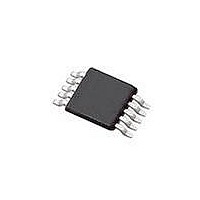
SI4010-C2-GT Silicon Laboratories Inc, SI4010-C2-GT Datasheet - Page 124

SI4010-C2-GT
Manufacturer Part Number
SI4010-C2-GT
Description
IC TX 27-960MHZ FSK 3.6V 10MSOP
Manufacturer
Silicon Laboratories Inc
Series
EZRadio®r
Type
Crystalless SoC RF Transmitterr
Datasheet
1.SI4010-C2-GT.pdf
(156 pages)
Specifications of SI4010-C2-GT
Package / Case
10-MSOP
Mfg Application Notes
SI4010 Calculator Spreadsheet AppNote
Frequency
27MHz ~ 960MHz
Applications
Garage Openers, RKE, Security Alarms
Modulation Or Protocol
FSK, OOK
Data Rate - Maximum
100 kBaud
Power - Output
10dBm
Current - Transmitting
19.8mA
Data Interface
PCB, Surface Mount
Antenna Connector
PCB, Surface Mount
Memory Size
4kB RAM
Features
8051 MCU Core, Crystal-less Operation
Voltage - Supply
1.8 V ~ 3.6 V
Operating Temperature
-40°C ~ 85°C
Operating Frequency
27 MHz to 960 MHz
Maximum Operating Temperature
+ 85 C
Mounting Style
SMD/SMT
Operating Supply Voltage
1.8 V to 3.6 V
Supply Current
14.2 mA
Lead Free Status / RoHS Status
Lead free / RoHS Compliant
Lead Free Status / RoHS Status
Lead free / RoHS Compliant, Lead free / RoHS Compliant
Other names
336-1997-5
Available stocks
Company
Part Number
Manufacturer
Quantity
Price
Part Number:
SI4010-C2-GT
Manufacturer:
SILICON LABS/èٹ¯ç§‘
Quantity:
20 000
Company:
Part Number:
SI4010-C2-GTR
Manufacturer:
ST
Quantity:
1 000
Part Number:
SI4010-C2-GTR
Manufacturer:
SILICON LABS/èٹ¯ç§‘
Quantity:
20 000
Si4010-C2
31.1. Register Description
SFR Definition 31.1. CLKOUT_SET
SFR Address = 0x8F
124
Name CLKOUT_
Reset
Bit
Type
7
6
Bit
CLKOUT_
CLKOUT_
Name
CLR
INV
CLR
R/W
7
0
CLKOUT Clear.
Write 1 to this bit clears the generated clock divider. The generated clock output is
forced to 0.
Reading this bit has CLKOUT_IDLE meaning. If read as 1 then it indicates that the
clock divider generator is idle. It can be used to wait for the clock to get idle after the
user clock output was disabled by PORT_SET.PORT_CLKEN=0. If this bit is read as
0 the clock division generator by factor 2 and above is running and the current user
clock period is still in progress.
The user could use this bit to synchronously switch the CLKOUT_DIV division factor,
but it is not necessary. The synchronous clock period switching is built in the hard-
ware. See the CLKOUT_DIV field description of this register. To switch the clocks
immediately without waiting for the current period to end, write 1 to this bit. The write
1 to this bit can be combined with setting the new CLKOUT_DIV value in this register
at the same time.
CLKOUT Inversion.
Invert the generated clock. The inverter is at the very end of the clock generation
chain. Normally, if this bit is 0, if the generated clock is disabled the output is at 0.
With this bit set to 1 the output is inverted, therefore the generated clock stops at 1.
This bit must be set before customer clock is enabled to the port output by setting
PORT_SET.PORT_CLKEN=1. If changed later the clock inversion takes effect imme-
diately with possibility of short clock pulse being generated at the clock output.
CLKOUT_
R/W
INV
6
0
CLKOUT_
SYM
R/W
5
0
R/W
Rev. 1.0
4
0
Function
R/W
3
0
CLKOUT_DIV[4:0]
R/W
2
0
R/W
1
0
R/W
0
0


