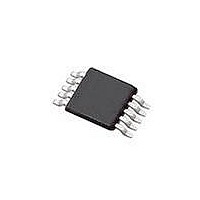
SI4010-C2-GT Silicon Laboratories Inc, SI4010-C2-GT Datasheet - Page 31

SI4010-C2-GT
Manufacturer Part Number
SI4010-C2-GT
Description
IC TX 27-960MHZ FSK 3.6V 10MSOP
Manufacturer
Silicon Laboratories Inc
Series
EZRadio®r
Type
Crystalless SoC RF Transmitterr
Datasheet
1.SI4010-C2-GT.pdf
(156 pages)
Specifications of SI4010-C2-GT
Package / Case
10-MSOP
Mfg Application Notes
SI4010 Calculator Spreadsheet AppNote
Frequency
27MHz ~ 960MHz
Applications
Garage Openers, RKE, Security Alarms
Modulation Or Protocol
FSK, OOK
Data Rate - Maximum
100 kBaud
Power - Output
10dBm
Current - Transmitting
19.8mA
Data Interface
PCB, Surface Mount
Antenna Connector
PCB, Surface Mount
Memory Size
4kB RAM
Features
8051 MCU Core, Crystal-less Operation
Voltage - Supply
1.8 V ~ 3.6 V
Operating Temperature
-40°C ~ 85°C
Operating Frequency
27 MHz to 960 MHz
Maximum Operating Temperature
+ 85 C
Mounting Style
SMD/SMT
Operating Supply Voltage
1.8 V to 3.6 V
Supply Current
14.2 mA
Lead Free Status / RoHS Status
Lead free / RoHS Compliant
Lead Free Status / RoHS Status
Lead free / RoHS Compliant, Lead free / RoHS Compliant
Other names
336-1997-5
Available stocks
Company
Part Number
Manufacturer
Quantity
Price
Part Number:
SI4010-C2-GT
Manufacturer:
SILICON LABS/èٹ¯ç§‘
Quantity:
20 000
Company:
Part Number:
SI4010-C2-GTR
Manufacturer:
ST
Quantity:
1 000
Part Number:
SI4010-C2-GTR
Manufacturer:
SILICON LABS/èٹ¯ç§‘
Quantity:
20 000
Table 10.5. Low Battery Detector Characteristics
(TA = 25° C, VDD = 3.3 V, RL = 480, unless otherwise noted)
Table 10.6. Optional Crystal Oscillator Characteristics
(TA = 25° C, VDD = 3.3 V, RL = 480, unless otherwise noted)
Table 10.4. Si4010 RF Transmitter Characteristics(Continued)
(TA = 25° C, VDD = 3.3 V, RL = 480,, SOIC package unless otherwise noted)
Parameter
Crystal Frequency Range
Input Capacitance (GPIO0)
Crystal ESR
Start-up Time
Parameter
Battery Voltage Measurement
Accuracy
Parameter
Peak to Peak
FSK Deviation
OOK Modulation depth
Antenna Tuning Capaci-
tive Range (Differential)
NVM Copy Boot Time
per kB
Notes:
1. The frequency range is continuous over the specified range.
2. The frequency step size is limited by the frequency noise.
3. Optimum differential load is equal to 3.5 V/(11.5 mA/2 x 4/PI) = 480 Therefore the antenna load resistance
4. Total NVM copy time = 2 ms + (NVM copy Boot Time per kB) x (NVM data in kB).
4
in parallel with the Si4010 differential output resistance should equal 480
Symbol
Symbol
Symbol
Max frequency deviation
GPIO0 configured as a crystal
GPIO0 configured as a crystal
GPIO0 configured as a crystal
GPIO0 configured as a crystal
oscillator; Crystal at Max ESR
GPI00 configured as a crystal
GPIO0 configured as crystal
oscillator; XO_LOWCAP=1
oscillator; XO_LOWCAP=0
oscillator; XO_LOWCAP=1
oscillator; XO_LOWCAP=0
Deviation resolution
Deviation accuracy
Test Condition
315 MHz
Rev. 1.0
Test Condition
Test Condition
oscillator
±(4 ppm + 2% pk-pk target
Min
2.4
—
—
—
60
FSK deviation in ppm)
Min
—
Min
10
—
—
—
—
—
Typ
275
3.6
—
—
2
Typ
Typ
5.5
Si4010-C2
2
—
—
—
3
9
Max
12.5
—
—
—
—
Max
Max
120
—
13
80
50
—
—
Unit
ppm
ppm
ppm
ms/
dB
pF
kB
Unit
MHz
Unit
ms
pF
pF
%
31


