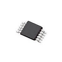
SI4010-C2-GT Silicon Laboratories Inc, SI4010-C2-GT Datasheet - Page 40

SI4010-C2-GT
Manufacturer Part Number
SI4010-C2-GT
Description
IC TX 27-960MHZ FSK 3.6V 10MSOP
Manufacturer
Silicon Laboratories Inc
Series
EZRadio®r
Type
Crystalless SoC RF Transmitterr
Datasheet
1.SI4010-C2-GT.pdf
(156 pages)
Specifications of SI4010-C2-GT
Package / Case
10-MSOP
Mfg Application Notes
SI4010 Calculator Spreadsheet AppNote
Frequency
27MHz ~ 960MHz
Applications
Garage Openers, RKE, Security Alarms
Modulation Or Protocol
FSK, OOK
Data Rate - Maximum
100 kBaud
Power - Output
10dBm
Current - Transmitting
19.8mA
Data Interface
PCB, Surface Mount
Antenna Connector
PCB, Surface Mount
Memory Size
4kB RAM
Features
8051 MCU Core, Crystal-less Operation
Voltage - Supply
1.8 V ~ 3.6 V
Operating Temperature
-40°C ~ 85°C
Operating Frequency
27 MHz to 960 MHz
Maximum Operating Temperature
+ 85 C
Mounting Style
SMD/SMT
Operating Supply Voltage
1.8 V to 3.6 V
Supply Current
14.2 mA
Lead Free Status / RoHS Status
Lead free / RoHS Compliant
Lead Free Status / RoHS Status
Lead free / RoHS Compliant, Lead free / RoHS Compliant
Other names
336-1997-5
Available stocks
Company
Part Number
Manufacturer
Quantity
Price
Part Number:
SI4010-C2-GT
Manufacturer:
SILICON LABS/èٹ¯ç§‘
Quantity:
20 000
Company:
Part Number:
SI4010-C2-GTR
Manufacturer:
ST
Quantity:
1 000
Part Number:
SI4010-C2-GTR
Manufacturer:
SILICON LABS/èٹ¯ç§‘
Quantity:
20 000
Si4010-C2
13. Output Data Serializer (ODS)
13.1. Description
The ODS block is responsible for synchronizing the output data to the required data rate and maintaining a
steady data flow during transmission. The serializer accomplishes the following functions:
The SFR and XREG settings of this block are determined from the desired modulation, data rate, and
encoding method and are automatically set by the ODS API in conjunction with the calculator. Users are
recommended to use the ODS API module functions for setting these registers.
13.2. Timing
40
(
L C _ E N A
P A _ L V L _ N S L I C E [ 4 : 0 ]
D I V _ E N A
P A _ E N A
L C _ E N A
F S K _ S H IF T [6 :0 ]
P A _ L V L _ N S L IC E [4 :0 ]
D IV _ E N A
P A _ E N A
Controls the edge rate of the PA on/off transitions.
Schedules PA, DIVIDER, LCOSC on/off power transitions for minimal power consumption.
Controls the serial data rate.
Provides handshake interface and a 1 byte pipeline to allow a software process to maintain steady
dataflow.
Modulates a 7 bit “frequency deviation” bus to the LC oscillator to allow for FSK operation.
Provides test features to force on the power state of the LCOSC, DIVIDER, and PA; recirculating a fixed
pattern; forcing the FSK offset frequency.
C O
L C _ W A R M U P
D I V _ W A R M U P
P A _ W A R M U P
Figure 13.1. OOK Timing Example
Figure 13.2. FSK Timing Example
f
Rev. 1.0
f
S Y M B O L T I M E
E D G E T I M E
f
O S )


