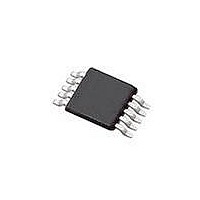
SI4010-C2-GT Silicon Laboratories Inc, SI4010-C2-GT Datasheet - Page 28

SI4010-C2-GT
Manufacturer Part Number
SI4010-C2-GT
Description
IC TX 27-960MHZ FSK 3.6V 10MSOP
Manufacturer
Silicon Laboratories Inc
Series
EZRadio®r
Type
Crystalless SoC RF Transmitterr
Datasheet
1.SI4010-C2-GT.pdf
(156 pages)
Specifications of SI4010-C2-GT
Package / Case
10-MSOP
Mfg Application Notes
SI4010 Calculator Spreadsheet AppNote
Frequency
27MHz ~ 960MHz
Applications
Garage Openers, RKE, Security Alarms
Modulation Or Protocol
FSK, OOK
Data Rate - Maximum
100 kBaud
Power - Output
10dBm
Current - Transmitting
19.8mA
Data Interface
PCB, Surface Mount
Antenna Connector
PCB, Surface Mount
Memory Size
4kB RAM
Features
8051 MCU Core, Crystal-less Operation
Voltage - Supply
1.8 V ~ 3.6 V
Operating Temperature
-40°C ~ 85°C
Operating Frequency
27 MHz to 960 MHz
Maximum Operating Temperature
+ 85 C
Mounting Style
SMD/SMT
Operating Supply Voltage
1.8 V to 3.6 V
Supply Current
14.2 mA
Lead Free Status / RoHS Status
Lead free / RoHS Compliant
Lead Free Status / RoHS Status
Lead free / RoHS Compliant, Lead free / RoHS Compliant
Other names
336-1997-5
Available stocks
Company
Part Number
Manufacturer
Quantity
Price
Part Number:
SI4010-C2-GT
Manufacturer:
SILICON LABS/èٹ¯ç§‘
Quantity:
20 000
Company:
Part Number:
SI4010-C2-GTR
Manufacturer:
ST
Quantity:
1 000
Part Number:
SI4010-C2-GTR
Manufacturer:
SILICON LABS/èٹ¯ç§‘
Quantity:
20 000
Table 10.2. Absolute Maximum Ratings
Si4010-C2
10. Electrical Characteristics
Table 10.1. Recommended Operating Conditions
28
Parameter
Supply Voltage
Input Current
Input Voltage
Junction Temperature
Storage Temperature
Notes:
Parameter
Supply Voltage
Supply Voltage Slew Rate
Ambient Temperature
Digital Input Range
*Note: Recommend bypass capacitor = 1 µF; slew rate measured 1 V < V
1. Permanent device damage may occur if the absolute maximum ratings are exceeded. Functional operation
2. Handling and assembly of these devices should only be done at ESD-protected workstations.
3. All input pins besides V
4. For GPIO pins configured as inputs.
should be restricted to the conditions as specified in the operational sections of this data sheet. Exposure
beyond recommended operating conditions for extended periods may affect device reliability.
3
4
DD
.
Symbol
V
T
DD
A
Symbol
T
V
V
I
T
STG
Initial Battery Insertion*
DD
IN
IN
J
1,2
Digital Input Signals
Test Condition
Rev. 1.0
–0.3 to (V
–0.5 to 3.9
–55 to 150
–40 to 90
Value
DD
10
DD
,< 1.7 V.
–0.3
+ 0.3)
Min
1.8
–40
20
Typ
—
—
25
—
V
Max
Unit
650
mA
3.6
0.3
DD
C
C
85
V
V
+
Unit
mV/
us
°C
V
V


