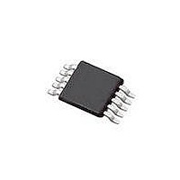
SI4010-C2-GT Silicon Laboratories Inc, SI4010-C2-GT Datasheet - Page 30

SI4010-C2-GT
Manufacturer Part Number
SI4010-C2-GT
Description
IC TX 27-960MHZ FSK 3.6V 10MSOP
Manufacturer
Silicon Laboratories Inc
Series
EZRadio®r
Type
Crystalless SoC RF Transmitterr
Datasheet
1.SI4010-C2-GT.pdf
(156 pages)
Specifications of SI4010-C2-GT
Package / Case
10-MSOP
Mfg Application Notes
SI4010 Calculator Spreadsheet AppNote
Frequency
27MHz ~ 960MHz
Applications
Garage Openers, RKE, Security Alarms
Modulation Or Protocol
FSK, OOK
Data Rate - Maximum
100 kBaud
Power - Output
10dBm
Current - Transmitting
19.8mA
Data Interface
PCB, Surface Mount
Antenna Connector
PCB, Surface Mount
Memory Size
4kB RAM
Features
8051 MCU Core, Crystal-less Operation
Voltage - Supply
1.8 V ~ 3.6 V
Operating Temperature
-40°C ~ 85°C
Operating Frequency
27 MHz to 960 MHz
Maximum Operating Temperature
+ 85 C
Mounting Style
SMD/SMT
Operating Supply Voltage
1.8 V to 3.6 V
Supply Current
14.2 mA
Lead Free Status / RoHS Status
Lead free / RoHS Compliant
Lead Free Status / RoHS Status
Lead free / RoHS Compliant, Lead free / RoHS Compliant
Other names
336-1997-5
Available stocks
Company
Part Number
Manufacturer
Quantity
Price
Part Number:
SI4010-C2-GT
Manufacturer:
SILICON LABS/èٹ¯ç§‘
Quantity:
20 000
Company:
Part Number:
SI4010-C2-GTR
Manufacturer:
ST
Quantity:
1 000
Part Number:
SI4010-C2-GTR
Manufacturer:
SILICON LABS/èٹ¯ç§‘
Quantity:
20 000
Si4010-C2
30
Table 10.4. Si4010 RF Transmitter Characteristics
(TA = 25° C, VDD = 3.3 V, RL = 480,, SOIC package unless otherwise noted)
Parameter
Frequency Range
Frequency Noise (rms)
Phase Noise @ 915 MHz
Frequency Tuning Time
Carrier Frequency
Accuracy
Transmit Power
Notes:
Frequency Error
Contribution with
External Crystal
PA Edge Ramp Rate
Programmable Range
Data Rate
1. The frequency range is continuous over the specified range.
2. The frequency step size is limited by the frequency noise.
3. Optimum differential load is equal to 3.5 V/(11.5 mA/2 x 4/PI) = 480 Therefore the antenna load resistance
4. Total NVM copy time = 2 ms + (NVM copy Boot Time per kB) x (NVM data in kB).
in parallel with the Si4010 differential output resistance should equal 480
3
1
2
Symbol
F
RF
power, with optimum differen-
power, with optimum differen-
differential load, V
Power variation vs temp and
Power variation vs temp and
differential load, V
OOK, Manchester encoding
Maximum programmed TX
Allen deviation, measured
Minimum programmed TX
Transmit power step size
tial load, V
supply, with optimum
supply, with optimum
across 1 ms interval
–40 °C ≤ T
from –13 to 10 dBm
FSK, NRZ encoding
0 °C ≤ T
Test Condition
100 kHz offset
10 kHz offset
1 MHz offset
V
OOK mode
Rev. 1.0
DD
tial load,
> 2.2 V
A
DD
A
≤ 70° C
≤ 85° C
> 2.2 V
DD
DD
> 2.2 V
> 1.8 V
–150
–250
–1.0
–2.5
0.34
Min
–10
0.1
0.1
27
—
—
—
—
—
—
—
—
–100
–105
0.25
Typ
–70
–13
0.3
10
—
—
—
—
—
—
—
—
—
5
+150
+250
Max
10.7
960
+10
100
0.5
0.5
50
—
—
—
—
—
—
—
—
dBc/Hz
dBc/Hz
dBc/Hz
kBaud
kBaud
MHz
dBm
dBm
Unit
ppm
ppm
ppm
ppm
ms
dB
dB
dB
us


