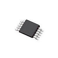
SI4010-C2-GT Silicon Laboratories Inc, SI4010-C2-GT Datasheet - Page 66

SI4010-C2-GT
Manufacturer Part Number
SI4010-C2-GT
Description
IC TX 27-960MHZ FSK 3.6V 10MSOP
Manufacturer
Silicon Laboratories Inc
Series
EZRadio®r
Type
Crystalless SoC RF Transmitterr
Datasheet
1.SI4010-C2-GT.pdf
(156 pages)
Specifications of SI4010-C2-GT
Package / Case
10-MSOP
Mfg Application Notes
SI4010 Calculator Spreadsheet AppNote
Frequency
27MHz ~ 960MHz
Applications
Garage Openers, RKE, Security Alarms
Modulation Or Protocol
FSK, OOK
Data Rate - Maximum
100 kBaud
Power - Output
10dBm
Current - Transmitting
19.8mA
Data Interface
PCB, Surface Mount
Antenna Connector
PCB, Surface Mount
Memory Size
4kB RAM
Features
8051 MCU Core, Crystal-less Operation
Voltage - Supply
1.8 V ~ 3.6 V
Operating Temperature
-40°C ~ 85°C
Operating Frequency
27 MHz to 960 MHz
Maximum Operating Temperature
+ 85 C
Mounting Style
SMD/SMT
Operating Supply Voltage
1.8 V to 3.6 V
Supply Current
14.2 mA
Lead Free Status / RoHS Status
Lead free / RoHS Compliant
Lead Free Status / RoHS Status
Lead free / RoHS Compliant, Lead free / RoHS Compliant
Other names
336-1997-5
Available stocks
Company
Part Number
Manufacturer
Quantity
Price
Part Number:
SI4010-C2-GT
Manufacturer:
SILICON LABS/èٹ¯ç§‘
Quantity:
20 000
Company:
Part Number:
SI4010-C2-GTR
Manufacturer:
ST
Quantity:
1 000
Part Number:
SI4010-C2-GTR
Manufacturer:
SILICON LABS/èٹ¯ç§‘
Quantity:
20 000
Si4010-C2
23.1. Program Memory
Program memory consists of 4.5 kB for RAM and 12 kB of ROM. The device employs a unified
CODE/XDATA RAM memory. On 8051 architecture the external data memory (XDATA) space is physically
different from the program memory (CODE); they can be accessed with different instructions. On this
device the RAM can store both CODE and XDATA at any location. The program memory is commonly
called CODE memory, residing in CODE address space.
Both MOVC and MOVX instructions can be used to read data from the CODE/XDATA address space.
The ROM holds the Silicon Labs proprietary code and cannot be read by a user. Only code can be exe-
cuted from ROM. If read is attempted by MOVC or MOVX instructions from ROM area the read value is
undetermined. The NVM and MTP memories are not mapped to the CPU address space.
23.2. Internal Data Memory
The device implements 256 bytes of internal RAM mapped into the data memory space from 0x00 through
0xFF. The lower 128 bytes of data memory are used for general purpose registers and memory. Either
direct or indirect addressing may be used to access the lower 128 bytes of data memory. Locations 0x00
through 0x1F are addressable as four banks of general purpose registers, each bank consisting of eight
byte-wide registers. The next 16 bytes, locations 0x20 through 0x2F, may either be addressed as bytes or
as 128 bit locations accessible with the direct addressing mode.
The upper 128 bytes of data memory are accessible only by indirect addressing. This region occupies the
same address space as the Special Function Registers (SFR) but is physically separate from the SFR
space. The addressing mode used by an instruction when accessing locations above 0x7F determines
whether the CPU accesses the upper 128 bytes of data memory space or the SFRs. Instructions that use
direct addressing will access the SFR space. Instructions using indirect addressing above 0x7F access the
upper 128 bytes of data memory. Figure 23.1 illustrates the data memory organization.
23.3. External Data Memory
Even though it is called external memory, it resides on the chip. This is the data memory, up to 64 kB in
size, which is accessible by MOVX instructions. For the original MCS-51™ architecture this memory
resided physically external to the chip. This memory is commonly referred as XDATA memory.
The device implements shared CODE/XDATA memory. The 4.5 kB of RAM is shared between the CODE
and XDATA. The CPU can run code from any location of that RAM, can read any location using MOVC and
MOVX instructions, and can write any location by using MOVX instruction.
Important note: Linker of the user application has to be given proper regions of CODE and XDATA mem-
ory, which are mutually exclusive. Therefore, for example, the user cannot set the CODE region to be
0x0000 .. 0x1000 and XDATA region to be the very same at the same time. One has to specify two non-
overlapping regions in the RAM area instead.
23.4. General Purpose Registers
The lower 32 bytes of data memory, locations 0x00 through 0x1F, may be addressed as four banks of gen-
eral-purpose registers. Each bank consists of eight byte-wide registers designated R0 through R7. Only
one of these banks may be enabled at a time. Two bits in the program status word, RS0 (PSW.3) and RS1
(PSW.4), select the active register bank. This allows fast context switching when entering subroutines and
interrupt service routines. Indirect addressing modes use registers R0 and R1 as index registers.
66
Rev. 1.0


