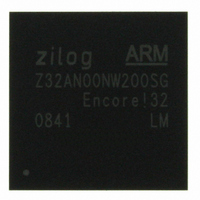
Z32AN00NW200SG Zilog, Z32AN00NW200SG Datasheet - Page 158

Z32AN00NW200SG
Manufacturer Part Number
Z32AN00NW200SG
Description
IC ARM922T MCU 200MHZ 256-BGA
Manufacturer
Zilog
Series
Encore!® 32r
Datasheet
1.Z32AN00NW200SG.pdf
(196 pages)
Specifications of Z32AN00NW200SG
Core Processor
ARM9
Core Size
16/32-Bit
Speed
200MHz
Connectivity
EBI/EMI, IrDA, SmartCard, SPI, UART/USART, USB OTG
Peripherals
DMA, LCD, Magnetic Card Reader, POR, PWM, WDT
Number Of I /o
76
Program Memory Type
ROMless
Ram Size
64K x 8
Voltage - Supply (vcc/vdd)
1.71 V ~ 3.6 V
Data Converters
A/D 4x10b
Oscillator Type
Internal
Operating Temperature
-40°C ~ 85°C
Package / Case
256-LBGA
For Use With
269-4713 - KIT DEV ENCORE 32 SERIES
Lead Free Status / RoHS Status
Lead free / RoHS Compliant
Eeprom Size
-
Program Memory Size
-
Other names
269-4717
Available stocks
Company
Part Number
Manufacturer
Quantity
Price
- Current page: 158 of 196
- Download datasheet (4Mb)
Z32AN Series Data Sheet
18.2.4 Slave Select (nSS)
18.3 Clock Phase and Polarity Control
18.3.1 Transfer Format (SPI_CTL.PHASE = 0)
DS0200-003
SCK and is sampled on the opposite edge where data is stable. Edge polarity is determined by the SPI
phase and polarity control.
This active low signal selects a slave device. In a system with multiple slaves, the master provides separate
nSS signals to each slave. nSS must be low prior to all data communication to and from the slave low for the
full duration of each character transferred. It can stay low during the transfer of multiple characters or may
de-assert between each character.
The SPI supports four combinations of clock phase and polarity using SPI_CTL.CLKPOL and
SPI_CTL.PHASE, as shown in the table below. For proper data transmission, the clock phase and polarity
must be identical for the SPI master and slave. The master always places data on the MOSI line a half-cycle
before the clock edge (SCK signal), in order for the slave to latch the data.
Figure 18-4 shows the timing diagram for 16-bit transfer in which SPI_CTL.PHASE is cleared. The two SCK
waveforms show both polarities of SPI_CTL.CLKPOL. In the case of multi-character transfers with nSS
remaining asserted between characters, the output data will change at the end of the Bit0 (final clock edge)
to reflect the output value for Bit15 of the next character.
Single Master SPI System: nSS is configured as an output by setting SPI_MOD.SSIO to ‘1’.
For communication between the master and slave devices, nSS controls the nSS input pin on
one of the Slave devices via SPI_MOD.SSV. GPIO output pins must be employed to select
additional SPI Slave devices when there are multiple Slaves.
Slave SPI System: nSS configured as an input by clearing SPI_MOD.SSIO to ‘0’.
Multi-Master SPI Systems: nSS pin must be configured as an input by clearing
SPI_MOD.SSIO to ‘0’. Other GPIO output pins are employed to select slave devices. When
acting as the master, if nSS goes low indicating another master is selecting this device as a
slave, SPI_STAT.COL is set, indicating a collision. The block is switched between master and
slave via SPI_CTL.MMEN.
PHASE
0
0
1
1
CLKPOL
0
1
0
1
SCK Transmit Edge
Falling
Falling
Rising
Rising
SCK Receive Edge
Falling
Falling
Rising
Rising
SCK Idle State
High
High
Low
Low
Page 145
Related parts for Z32AN00NW200SG
Image
Part Number
Description
Manufacturer
Datasheet
Request
R

Part Number:
Description:
Communication Controllers, ZILOG INTELLIGENT PERIPHERAL CONTROLLER (ZIP)
Manufacturer:
Zilog, Inc.
Datasheet:

Part Number:
Description:
KIT DEV FOR Z8 ENCORE 16K TO 64K
Manufacturer:
Zilog
Datasheet:

Part Number:
Description:
KIT DEV Z8 ENCORE XP 28-PIN
Manufacturer:
Zilog
Datasheet:

Part Number:
Description:
DEV KIT FOR Z8 ENCORE 8K/4K
Manufacturer:
Zilog
Datasheet:

Part Number:
Description:
KIT DEV Z8 ENCORE XP 28-PIN
Manufacturer:
Zilog
Datasheet:

Part Number:
Description:
DEV KIT FOR Z8 ENCORE 4K TO 8K
Manufacturer:
Zilog
Datasheet:

Part Number:
Description:
CMOS Z8 microcontroller. ROM 16 Kbytes, RAM 256 bytes, speed 16 MHz, 32 lines I/O, 3.0V to 5.5V
Manufacturer:
Zilog, Inc.
Datasheet:

Part Number:
Description:
Low-cost microcontroller. 512 bytes ROM, 61 bytes RAM, 8 MHz
Manufacturer:
Zilog, Inc.
Datasheet:

Part Number:
Description:
Z8 4K OTP Microcontroller
Manufacturer:
Zilog, Inc.
Datasheet:

Part Number:
Description:
CMOS SUPER8 ROMLESS MCU
Manufacturer:
Zilog, Inc.
Datasheet:

Part Number:
Description:
SL1866 CMOSZ8 OTP Microcontroller
Manufacturer:
Zilog, Inc.
Datasheet:

Part Number:
Description:
SL1866 CMOSZ8 OTP Microcontroller
Manufacturer:
Zilog, Inc.
Datasheet:

Part Number:
Description:
OTP (KB) = 1, RAM = 125, Speed = 12, I/O = 14, 8-bit Timers = 2, Comm Interfaces Other Features = Por, LV Protect, Voltage = 4.5-5.5V
Manufacturer:
Zilog, Inc.
Datasheet:

Part Number:
Description:
Manufacturer:
Zilog, Inc.
Datasheet:


