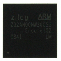
Z32AN00NW200SG Zilog, Z32AN00NW200SG Datasheet - Page 43

Z32AN00NW200SG
Manufacturer Part Number
Z32AN00NW200SG
Description
IC ARM922T MCU 200MHZ 256-BGA
Manufacturer
Zilog
Series
Encore!® 32r
Datasheet
1.Z32AN00NW200SG.pdf
(196 pages)
Specifications of Z32AN00NW200SG
Core Processor
ARM9
Core Size
16/32-Bit
Speed
200MHz
Connectivity
EBI/EMI, IrDA, SmartCard, SPI, UART/USART, USB OTG
Peripherals
DMA, LCD, Magnetic Card Reader, POR, PWM, WDT
Number Of I /o
76
Program Memory Type
ROMless
Ram Size
64K x 8
Voltage - Supply (vcc/vdd)
1.71 V ~ 3.6 V
Data Converters
A/D 4x10b
Oscillator Type
Internal
Operating Temperature
-40°C ~ 85°C
Package / Case
256-LBGA
For Use With
269-4713 - KIT DEV ENCORE 32 SERIES
Lead Free Status / RoHS Status
Lead free / RoHS Compliant
Eeprom Size
-
Program Memory Size
-
Other names
269-4717
Available stocks
Company
Part Number
Manufacturer
Quantity
Price
- Current page: 43 of 196
- Download datasheet (4Mb)
Z32AN Series Data Sheet
7.1.1.4
DS0200-003
The default memory range for CS0 is16MB or 128Mb is extended to 32MB by using the CS1 address space.
MEMC_CFG_1.EXT has been added for CS1 and CS3 only. When ‘0’, CS0 is ‘0’ from address 10000000h –
10FFFFFFh (16MB) as presently specified. When EXT is ‘1’ for CS1, CS0 is ‘0’ for addresses 10000000h –
11FFFFFFh or 32MB (256Mb) and CS1 becomes the 25th address bit, A[24], for either the primary or
secondary bus depending on programmable selection. The CS1 pin as A[24] is inverted. When EXT is ‘1’ for
CS3, CS0 is ‘0’ for addresses 10000000h - 10FFFFFFh and 13000000h – 13FFFFFFh or 32MB (256Mb)
and CS3 becomes the 25th address bit, A[24], for either the primary or secondary bus depending on
programmable selection. The CS3 pin as A[24] is inverted.
To use CS1 or CS3 as A[24], an inverter may be added to the output of this signal to address the larger
256Mb memory device.
Operation is the same for CS1 of CS3 except for the address space. CS1 is used here to explain the
function. After reset, the boot ROM reads CS0 which sets CS0 =0 and CS1= 1 (default memory
configuration). The inverter will drive A24 low, placing the start of the larger memory at 10000000h. The boot
ROM checks memory for a valid boot image and if valid, control is turned over to this memory.
When a larger memory device is used (256Mb) then the user code must set MEMC_CFG_1.EXT to ‘1’, to
extend the memory range for CS0. This must be done within the first 16MB or 128Mbits of code space.
After MEMC_CFG_1.EXT is set to ‘1’, CS0 is ‘0’ for the entire address space 10000000h – 11FFFFFFh.
CS1 is ‘0’ for address spaces 11000000h – 11FFFFFFh. The rest of the time CS1 is ‘1’. Since CS1 behaves
as an inverted address bit going into the memory, the external inverter on CS1 will cause correct behavior of
A[24] for the address space 10000000h – 11FFFFFFh.
Extending CS0 memory space
Figure 7-1: CS1 as A[24]
Page 30
Related parts for Z32AN00NW200SG
Image
Part Number
Description
Manufacturer
Datasheet
Request
R

Part Number:
Description:
Communication Controllers, ZILOG INTELLIGENT PERIPHERAL CONTROLLER (ZIP)
Manufacturer:
Zilog, Inc.
Datasheet:

Part Number:
Description:
KIT DEV FOR Z8 ENCORE 16K TO 64K
Manufacturer:
Zilog
Datasheet:

Part Number:
Description:
KIT DEV Z8 ENCORE XP 28-PIN
Manufacturer:
Zilog
Datasheet:

Part Number:
Description:
DEV KIT FOR Z8 ENCORE 8K/4K
Manufacturer:
Zilog
Datasheet:

Part Number:
Description:
KIT DEV Z8 ENCORE XP 28-PIN
Manufacturer:
Zilog
Datasheet:

Part Number:
Description:
DEV KIT FOR Z8 ENCORE 4K TO 8K
Manufacturer:
Zilog
Datasheet:

Part Number:
Description:
CMOS Z8 microcontroller. ROM 16 Kbytes, RAM 256 bytes, speed 16 MHz, 32 lines I/O, 3.0V to 5.5V
Manufacturer:
Zilog, Inc.
Datasheet:

Part Number:
Description:
Low-cost microcontroller. 512 bytes ROM, 61 bytes RAM, 8 MHz
Manufacturer:
Zilog, Inc.
Datasheet:

Part Number:
Description:
Z8 4K OTP Microcontroller
Manufacturer:
Zilog, Inc.
Datasheet:

Part Number:
Description:
CMOS SUPER8 ROMLESS MCU
Manufacturer:
Zilog, Inc.
Datasheet:

Part Number:
Description:
SL1866 CMOSZ8 OTP Microcontroller
Manufacturer:
Zilog, Inc.
Datasheet:

Part Number:
Description:
SL1866 CMOSZ8 OTP Microcontroller
Manufacturer:
Zilog, Inc.
Datasheet:

Part Number:
Description:
OTP (KB) = 1, RAM = 125, Speed = 12, I/O = 14, 8-bit Timers = 2, Comm Interfaces Other Features = Por, LV Protect, Voltage = 4.5-5.5V
Manufacturer:
Zilog, Inc.
Datasheet:

Part Number:
Description:
Manufacturer:
Zilog, Inc.
Datasheet:


