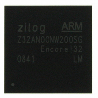
Z32AN00NW200SG Zilog, Z32AN00NW200SG Datasheet - Page 83

Z32AN00NW200SG
Manufacturer Part Number
Z32AN00NW200SG
Description
IC ARM922T MCU 200MHZ 256-BGA
Manufacturer
Zilog
Series
Encore!® 32r
Datasheet
1.Z32AN00NW200SG.pdf
(196 pages)
Specifications of Z32AN00NW200SG
Core Processor
ARM9
Core Size
16/32-Bit
Speed
200MHz
Connectivity
EBI/EMI, IrDA, SmartCard, SPI, UART/USART, USB OTG
Peripherals
DMA, LCD, Magnetic Card Reader, POR, PWM, WDT
Number Of I /o
76
Program Memory Type
ROMless
Ram Size
64K x 8
Voltage - Supply (vcc/vdd)
1.71 V ~ 3.6 V
Data Converters
A/D 4x10b
Oscillator Type
Internal
Operating Temperature
-40°C ~ 85°C
Package / Case
256-LBGA
For Use With
269-4713 - KIT DEV ENCORE 32 SERIES
Lead Free Status / RoHS Status
Lead free / RoHS Compliant
Eeprom Size
-
Program Memory Size
-
Other names
269-4717
Available stocks
Company
Part Number
Manufacturer
Quantity
Price
- Current page: 83 of 196
- Download datasheet (4Mb)
Z32AN Series Data Sheet
10.1.2 Reset and Power-up Management
10.1.3 Chip to Smart Card Interface Mapping
10.1.4 DMA Interface
10.1.5 Synchronous Smart Card Handling
10.1.6 Interrupt Generation
DS0200-003
When reset or power-up commands are issued using the COMMAND register, the controller transfers the
corresponding command words to the selected Smart Card through the SPI bus. The command request is
queued and sent through the SPI bus as soon as the current SPI transfer is complete. The voltage
information and clock division ratios must be programmed before the reset or power-up command is issued.
The SPI command format is (most significant bit first) is given below:
Where,
Smart Card 0 is mapped to the Maincard. Smart Card 1 communicates with a SIM via the interface device.
For the non-active Smart Card, the clock and I/O lines are held inactive. Which SIM to use is selected by
SIM_SEL. At reset, Smart Card 1 is mapped to SIM0 (deactivated).
Each DMA channel can be independently assigned to either of the Smart Card RX or TX channels or
deactivated. For example, the TX channel can be used with Smart Card 0 while the RX channel is used with
Smart Card 1. At reset, the RX and TX DMA channels are not mapped and must be configured prior to use.
The SPI interface allows management of synchronous Smart Cards by sending corresponding commands to
the interface devices to manually activate the clock and data signals.
Following are the interrupt sources:
These interrupt sources are combined to generate the Smart Card Alarm interrupt and can be individually
masked in SC_IMASK. The Smart Card interfaces also provide interrupts. These interrupts cannot be
masked in SC_IMASK. However, their status is available in SC_ISTAT.
►Note: Ensure that Smart Card 0 and Smart Card 1 are not mapped onto the same DMA channel
as it can lead to unpredictable operation.
S[2:0]: target Smart Card interface address (INT1=000, INT2=001 INT3=010, INT4=011, EXT
ASYNC=100).
nRST: is the active-Low reset signal to be applied to the Smart Card.
CK[1:0]: is the content of the CLKDIV register for the Smart Card.
VCC[1:0]: is the content of the VCC register for the active Smart Card when the card must be
powered on or 00 when the active card must be powered off.
SPI Interrupt: Occurs whenever an SPI collision occurs. For example, the CPU writes new
data into the SPIDATA register while the previous transfer is not
completed. Bit 8 of the SPIDATA register remains at 0 when the transfer is in process.
ALARM Interrupt: Occurs whenever one of the Smart Card interfaces generates an interrupt
indicating over current, overheating, card removal or card insertion is on one Smart Card
socket. The interrupt lines from each Smart Card interface are combined to form the
SC_nALARM.
ALARM TRIG Interrupt: Generated whenever a High to Low transition is detected on the
SC_nALARM input.
Page 70
Related parts for Z32AN00NW200SG
Image
Part Number
Description
Manufacturer
Datasheet
Request
R

Part Number:
Description:
Communication Controllers, ZILOG INTELLIGENT PERIPHERAL CONTROLLER (ZIP)
Manufacturer:
Zilog, Inc.
Datasheet:

Part Number:
Description:
KIT DEV FOR Z8 ENCORE 16K TO 64K
Manufacturer:
Zilog
Datasheet:

Part Number:
Description:
KIT DEV Z8 ENCORE XP 28-PIN
Manufacturer:
Zilog
Datasheet:

Part Number:
Description:
DEV KIT FOR Z8 ENCORE 8K/4K
Manufacturer:
Zilog
Datasheet:

Part Number:
Description:
KIT DEV Z8 ENCORE XP 28-PIN
Manufacturer:
Zilog
Datasheet:

Part Number:
Description:
DEV KIT FOR Z8 ENCORE 4K TO 8K
Manufacturer:
Zilog
Datasheet:

Part Number:
Description:
CMOS Z8 microcontroller. ROM 16 Kbytes, RAM 256 bytes, speed 16 MHz, 32 lines I/O, 3.0V to 5.5V
Manufacturer:
Zilog, Inc.
Datasheet:

Part Number:
Description:
Low-cost microcontroller. 512 bytes ROM, 61 bytes RAM, 8 MHz
Manufacturer:
Zilog, Inc.
Datasheet:

Part Number:
Description:
Z8 4K OTP Microcontroller
Manufacturer:
Zilog, Inc.
Datasheet:

Part Number:
Description:
CMOS SUPER8 ROMLESS MCU
Manufacturer:
Zilog, Inc.
Datasheet:

Part Number:
Description:
SL1866 CMOSZ8 OTP Microcontroller
Manufacturer:
Zilog, Inc.
Datasheet:

Part Number:
Description:
SL1866 CMOSZ8 OTP Microcontroller
Manufacturer:
Zilog, Inc.
Datasheet:

Part Number:
Description:
OTP (KB) = 1, RAM = 125, Speed = 12, I/O = 14, 8-bit Timers = 2, Comm Interfaces Other Features = Por, LV Protect, Voltage = 4.5-5.5V
Manufacturer:
Zilog, Inc.
Datasheet:

Part Number:
Description:
Manufacturer:
Zilog, Inc.
Datasheet:


