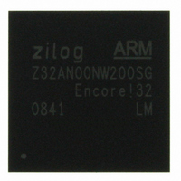
Z32AN00NW200SG Zilog, Z32AN00NW200SG Datasheet - Page 64

Z32AN00NW200SG
Manufacturer Part Number
Z32AN00NW200SG
Description
IC ARM922T MCU 200MHZ 256-BGA
Manufacturer
Zilog
Series
Encore!® 32r
Datasheet
1.Z32AN00NW200SG.pdf
(196 pages)
Specifications of Z32AN00NW200SG
Core Processor
ARM9
Core Size
16/32-Bit
Speed
200MHz
Connectivity
EBI/EMI, IrDA, SmartCard, SPI, UART/USART, USB OTG
Peripherals
DMA, LCD, Magnetic Card Reader, POR, PWM, WDT
Number Of I /o
76
Program Memory Type
ROMless
Ram Size
64K x 8
Voltage - Supply (vcc/vdd)
1.71 V ~ 3.6 V
Data Converters
A/D 4x10b
Oscillator Type
Internal
Operating Temperature
-40°C ~ 85°C
Package / Case
256-LBGA
For Use With
269-4713 - KIT DEV ENCORE 32 SERIES
Lead Free Status / RoHS Status
Lead free / RoHS Compliant
Eeprom Size
-
Program Memory Size
-
Other names
269-4717
Available stocks
Company
Part Number
Manufacturer
Quantity
Price
- Current page: 64 of 196
- Download datasheet (4Mb)
Z32AN Series Data Sheet
8.3
8.4
DS0200-003
Word
Data
Size
Size
16
32
16
32
8
Destination Device
8
Source Device
The table below depicts how data is moved into the DMA FIFO based on the settings of DMA_SRCN[1:0]
and DMA_CFGN.SWIDTH. If the width of the device is larger than the current value of DMA_CNTN, the
DMA Controller performs an AHB cycle to a smaller width.
Data Movement from the DMA FIFO to the Destination
The following registers and fields affect destination data movement of the DMA transfer:
The table below depicts how data is moved out of the FIFO based on the settings of
DMA_FIFO_COUNTER, DMA_DESTN[1:0] and DMA_CFGN.DWIDTH. If the width of the device is larger
than the number of bytes left in the FIFO, the DMA Controller performs an AHB cycle to a smaller width.
Memory Buffer Alignment
The DMA controller adjusts the transfer size to provide correct buffer alignment.
3
X
X
X
3
X
X
X
Active Bytes
Active Bytes
2
X
X
X
2
X
X
X
DMA_DESTN → All bits
DMA_CNTN → All bits
DMA_CFGN → BURST, DWIDTH, DINCR
1
X
X
X
1
X
X
X
0
X
X
X
0
X
X
X
DWIDTH
SWIDTH
1
0
0
1
1
0
0
1
Register Field Values
Register Field Values
0
0
0
1
0
0
1
0
DMA_SRCN
DMA_DESTN
1
0
0
1
1
0
1
0
1
0
0
1
1
0
1
0
Table 8-3: Outbound Data Alignment
Table 8-2: Inbound Data Alignment
0
0
1
0
1
0
0
0
0
0
1
0
1
0
0
0
One AHB byte read for each byte moved. Only data from the
indicated byte lane will be moved into the DMA FIFO (LS byte first).
One AHB half-word read for each half-word moved. Only data from
the indicated byte lanes will be moved into the DMA FIFO (least
significant half-word first).
One AHB word read for each word moved. The entire word is moved
into the DMA FIFO.
Resulting AHB Burst
One AHB byte write for each byte moved. Bytes will be moved out
of the DMA FIFO (LS byte first) onto the indicated byte lane.
One AHB half-word write for each half-word moved. Half-words will
be moved out of the DMA FIFO (least significant half-word first)
onto the indicated byte lanes.
One AHB word write for each word moved.
The entire word is moved out of the DMA FIFO.
Resulting AHB Burst
Page 51
Related parts for Z32AN00NW200SG
Image
Part Number
Description
Manufacturer
Datasheet
Request
R

Part Number:
Description:
Communication Controllers, ZILOG INTELLIGENT PERIPHERAL CONTROLLER (ZIP)
Manufacturer:
Zilog, Inc.
Datasheet:

Part Number:
Description:
KIT DEV FOR Z8 ENCORE 16K TO 64K
Manufacturer:
Zilog
Datasheet:

Part Number:
Description:
KIT DEV Z8 ENCORE XP 28-PIN
Manufacturer:
Zilog
Datasheet:

Part Number:
Description:
DEV KIT FOR Z8 ENCORE 8K/4K
Manufacturer:
Zilog
Datasheet:

Part Number:
Description:
KIT DEV Z8 ENCORE XP 28-PIN
Manufacturer:
Zilog
Datasheet:

Part Number:
Description:
DEV KIT FOR Z8 ENCORE 4K TO 8K
Manufacturer:
Zilog
Datasheet:

Part Number:
Description:
CMOS Z8 microcontroller. ROM 16 Kbytes, RAM 256 bytes, speed 16 MHz, 32 lines I/O, 3.0V to 5.5V
Manufacturer:
Zilog, Inc.
Datasheet:

Part Number:
Description:
Low-cost microcontroller. 512 bytes ROM, 61 bytes RAM, 8 MHz
Manufacturer:
Zilog, Inc.
Datasheet:

Part Number:
Description:
Z8 4K OTP Microcontroller
Manufacturer:
Zilog, Inc.
Datasheet:

Part Number:
Description:
CMOS SUPER8 ROMLESS MCU
Manufacturer:
Zilog, Inc.
Datasheet:

Part Number:
Description:
SL1866 CMOSZ8 OTP Microcontroller
Manufacturer:
Zilog, Inc.
Datasheet:

Part Number:
Description:
SL1866 CMOSZ8 OTP Microcontroller
Manufacturer:
Zilog, Inc.
Datasheet:

Part Number:
Description:
OTP (KB) = 1, RAM = 125, Speed = 12, I/O = 14, 8-bit Timers = 2, Comm Interfaces Other Features = Por, LV Protect, Voltage = 4.5-5.5V
Manufacturer:
Zilog, Inc.
Datasheet:

Part Number:
Description:
Manufacturer:
Zilog, Inc.
Datasheet:


