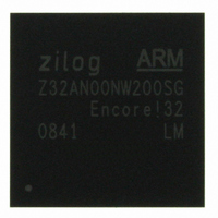
Z32AN00NW200SG Zilog, Z32AN00NW200SG Datasheet - Page 21

Z32AN00NW200SG
Manufacturer Part Number
Z32AN00NW200SG
Description
IC ARM922T MCU 200MHZ 256-BGA
Manufacturer
Zilog
Series
Encore!® 32r
Datasheet
1.Z32AN00NW200SG.pdf
(196 pages)
Specifications of Z32AN00NW200SG
Core Processor
ARM9
Core Size
16/32-Bit
Speed
200MHz
Connectivity
EBI/EMI, IrDA, SmartCard, SPI, UART/USART, USB OTG
Peripherals
DMA, LCD, Magnetic Card Reader, POR, PWM, WDT
Number Of I /o
76
Program Memory Type
ROMless
Ram Size
64K x 8
Voltage - Supply (vcc/vdd)
1.71 V ~ 3.6 V
Data Converters
A/D 4x10b
Oscillator Type
Internal
Operating Temperature
-40°C ~ 85°C
Package / Case
256-LBGA
For Use With
269-4713 - KIT DEV ENCORE 32 SERIES
Lead Free Status / RoHS Status
Lead free / RoHS Compliant
Eeprom Size
-
Program Memory Size
-
Other names
269-4717
Available stocks
Company
Part Number
Manufacturer
Quantity
Price
- Current page: 21 of 196
- Download datasheet (4Mb)
Z32AN Series Data Sheet
Chapter 3: System Clocks and Power Management
DS0200-003
Signal Name
CLKXI/CLKXO
The Z32AN Series contains a Power Management Unit (PMU) that controls system clocking and power
management. The configuration of the PMU is performed through the PMU registers. Upon a hard reset, the
PMU drives the main oscillator clock onto the system clock. All digital clock domains are enabled and most
analog circuits are powered down.
The PLL typically locks 100µs after it is enabled. The lock bit should be checked before switching clock
source to the PLL. After the PLL has locked, the programmer can write to the PMU registers to control clock
frequencies and clock gating. The PMU contains control circuits to allow for glitch-free, dynamic
configuration of all clocks. The boot ROM configures the PLL at start up.
gpio_wake
hclk[31:0]
rtc_wake
daaclk
sdclk
fclk
Dir
O
O
O
O
I
I
I
Description
Input/Output connection to the main external crystal. Any frequency from 14MHz-40MHz may be
used. A clock must be present for the device to come out of reset.
Main CPU clock.
System clocks. These clocks are driven to the AHB and APB devices as well as the AHB interface
of the CPU. This clock can be enabled or disabled on a module-by-module basis. (See PMU Clock
Enable Register (ADDR = 0xFFFF_E008)
Clock driven into the DAA. The DAA requires a 24.000MHz clock.
Clock eventually driven onto the CLKOUT pin. This signal first goes through the SDRAM Controller
module where it may be subject to additional clock gating.
Signal from GPIO to wake system upon any GPIO input transition. See Using the GPIO Wake
Function. Though shown as a single signal, there are wake signals from all GPIO modules.
Signal from RTC to wake system upon activation of the RTC alarm. See Real-Time Clock (RTC).
Table 3-1: PMU Module Inputs and Outputs
Figure 3-1: Simplified PMU Block Diagram
Page 8
Related parts for Z32AN00NW200SG
Image
Part Number
Description
Manufacturer
Datasheet
Request
R

Part Number:
Description:
Communication Controllers, ZILOG INTELLIGENT PERIPHERAL CONTROLLER (ZIP)
Manufacturer:
Zilog, Inc.
Datasheet:

Part Number:
Description:
KIT DEV FOR Z8 ENCORE 16K TO 64K
Manufacturer:
Zilog
Datasheet:

Part Number:
Description:
KIT DEV Z8 ENCORE XP 28-PIN
Manufacturer:
Zilog
Datasheet:

Part Number:
Description:
DEV KIT FOR Z8 ENCORE 8K/4K
Manufacturer:
Zilog
Datasheet:

Part Number:
Description:
KIT DEV Z8 ENCORE XP 28-PIN
Manufacturer:
Zilog
Datasheet:

Part Number:
Description:
DEV KIT FOR Z8 ENCORE 4K TO 8K
Manufacturer:
Zilog
Datasheet:

Part Number:
Description:
CMOS Z8 microcontroller. ROM 16 Kbytes, RAM 256 bytes, speed 16 MHz, 32 lines I/O, 3.0V to 5.5V
Manufacturer:
Zilog, Inc.
Datasheet:

Part Number:
Description:
Low-cost microcontroller. 512 bytes ROM, 61 bytes RAM, 8 MHz
Manufacturer:
Zilog, Inc.
Datasheet:

Part Number:
Description:
Z8 4K OTP Microcontroller
Manufacturer:
Zilog, Inc.
Datasheet:

Part Number:
Description:
CMOS SUPER8 ROMLESS MCU
Manufacturer:
Zilog, Inc.
Datasheet:

Part Number:
Description:
SL1866 CMOSZ8 OTP Microcontroller
Manufacturer:
Zilog, Inc.
Datasheet:

Part Number:
Description:
SL1866 CMOSZ8 OTP Microcontroller
Manufacturer:
Zilog, Inc.
Datasheet:

Part Number:
Description:
OTP (KB) = 1, RAM = 125, Speed = 12, I/O = 14, 8-bit Timers = 2, Comm Interfaces Other Features = Por, LV Protect, Voltage = 4.5-5.5V
Manufacturer:
Zilog, Inc.
Datasheet:

Part Number:
Description:
Manufacturer:
Zilog, Inc.
Datasheet:


