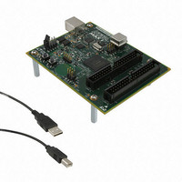
DK-DEV-5M570ZN Altera, DK-DEV-5M570ZN Datasheet - Page 10

DK-DEV-5M570ZN
Manufacturer Part Number
DK-DEV-5M570ZN
Description
KIT DEV MAX V 5M570Z
Manufacturer
Altera
Series
MAX® Vr
Type
CPLDr
Datasheets
1.DK-DEV-5M570ZN.pdf
(30 pages)
2.DK-DEV-5M570ZN.pdf
(2 pages)
3.DK-DEV-5M570ZN.pdf
(30 pages)
4.DK-DEV-5M570ZN.pdf
(164 pages)
5.DK-DEV-5M570ZN.pdf
(24 pages)
Specifications of DK-DEV-5M570ZN
Contents
Board, Cable(s), Software and Documentation
Silicon Manufacturer
Altera
Core Architecture
CPLD
Core Sub-architecture
MAX
Silicon Core Number
5M
Silicon Family Name
MAX V
Kit Contents
MAX V CPLD Development Board, USB Cable
Rohs Compliant
Yes
Lead Free Status / RoHS Status
Lead free / RoHS Compliant
For Use With/related Products
5M570ZF256
Lead Free Status / Rohs Status
Compliant
Other names
544-2722
Available stocks
Company
Part Number
Manufacturer
Quantity
Price
1–2
Table 1–1. MAX V Family Features
MAX V Device Handbook
Feature
LEs
Typical Equivalent Macrocells
User Flash Memory Size (bits)
Global Clocks
Internal Oscillator
Maximum User I/O pins
t
f
t
t
Notes to
(1) t
(2) The maximum global clock frequency, f
PD1
CNT
SU
CO
(ns)
(ns)
(ns)
(MHz)
implemented in a single LUT and LAB that is adjacent to the output pin.
than this number.
PD1
represents a pin-to-pin delay for the worst case I/O placement with a full diagonal path across the device and combinational logic
Table
(1)
(2)
1–1:
f
■
■
■
Table 1–1
MAX V devices accept 1.8 V on their VCCINT pins. The 1.8-V V
powers the device core directly. MAX V devices operate internally at 1.8 V. The
supported MultiVolt I/O interface voltage levels (V
and 3.3 V.
MAX V devices are available in two speed grades: –4 and –5, with –4 being the fastest.
For commercial applications, speed grades –C4 and –C5 are available. For industrial
applications, speed grade –I5 is available. These speed grades represent the overall
relative performance, not any specific timing parameter.
For propagation delay timing numbers within each speed grade and density, refer to
the
MAX V devices are available in space-saving FineLine BGA (FBGA), Micro FineLine
BGA (MBGA), plastic enhanced quad flat pack (EQFP), and thin quad flat pack
(TQFP) packages (refer to
migration within the same package (for example, you can migrate between the
5M570Z, 5M1270Z, and 5M2210Z devices in the 256-pin FineLine BGA package).
Vertical migration means that you can migrate to devices whose dedicated pins and
JTAG pins are the same and power pins are subsets or supersets for a given package
across device densities. The largest density in any package has the highest number of
power pins; you must lay out for the largest planned density in a package to provide
I/Os are fully compliant with the PCI-SIG
2.2 for 3.3-V operation
Hot-socket compliant
Built-in JTAG BST circuitry compliant with IEEE Std. 1149.1-1990
DC and Switching Characteristics for MAX V Devices
lists the MAX V family features.
5M40Z
8,192
CNT
152
7.5
2.3
6.5
40
32
54
4
1
, is limited by the I/O standard on the clock input pin. The 16-bit counter critical delay will run faster
5M80Z
8,192
152
7.5
2.3
6.5
80
64
79
4
1
Table 1–2
5M160Z
8,192
160
128
152
7.5
2.3
6.5
79
4
1
and
Table
5M240Z
8,192
®
240
192
114
152
7.5
2.3
6.5
1–3). MAX V devices support vertical
4
1
PCI Local Bus Specification, revision
CCIO
Chapter 1: MAX V Device Family Overview
chapter.
5M570Z
) are 1.2 V, 1.5 V, 1.8 V, 2.5 V,
8,192
159
570
440
152
9.0
2.2
6.7
4
1
January 2011 Altera Corporation
CCINT
5M1270Z
1,270
8,192
external supply
980
271
304
6.2
1.2
4.6
4
1
Feature Summary
5M2210Z
2,210
1,700
8,192
271
304
7.0
1.2
4.6
4
1


