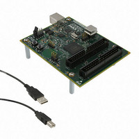
DK-DEV-5M570ZN Altera, DK-DEV-5M570ZN Datasheet - Page 160

DK-DEV-5M570ZN
Manufacturer Part Number
DK-DEV-5M570ZN
Description
KIT DEV MAX V 5M570Z
Manufacturer
Altera
Series
MAX® Vr
Type
CPLDr
Datasheets
1.DK-DEV-5M570ZN.pdf
(30 pages)
2.DK-DEV-5M570ZN.pdf
(2 pages)
3.DK-DEV-5M570ZN.pdf
(30 pages)
4.DK-DEV-5M570ZN.pdf
(164 pages)
5.DK-DEV-5M570ZN.pdf
(24 pages)
Specifications of DK-DEV-5M570ZN
Contents
Board, Cable(s), Software and Documentation
Silicon Manufacturer
Altera
Core Architecture
CPLD
Core Sub-architecture
MAX
Silicon Core Number
5M
Silicon Family Name
MAX V
Kit Contents
MAX V CPLD Development Board, USB Cable
Rohs Compliant
Yes
Lead Free Status / RoHS Status
Lead free / RoHS Compliant
For Use With/related Products
5M570ZF256
Lead Free Status / Rohs Status
Compliant
Other names
544-2722
Available stocks
Company
Part Number
Manufacturer
Quantity
Price
8–14
Boundary-Scan Test for Programmed Devices
MAX V Device Handbook
f
levels, the devices can interface with each other. For example, a device with 3.3-V
V
transistor-to-transistor logic (TTL)-level input for the 5.0-V V
on MAX V devices can support 1.5-, 1.8-, 2.5-, or 3.3-V input levels, depending on the
V
For more information about MultiVolt I/O support, refer to the
Architecture
You can interface the TDI and TDO lines of the JTAG pins of devices that have different
V
chain must be built such that a device with a higher V
an equal or lower V
shifter may be required only to shift the TDO level to a level acceptable to the JTAG
tester.
Figure 8–13
inserted in the chain.
Figure 8–13. JTAG Chain of Mixed Voltages
For a programmed device, the input buffers are turned off by default for I/O pins that
are set as output only in the design file. You cannot sample on the programmed device
output pins with the default boundary-scan description language (BSDL) file when
the input buffers are turned off.
For boundary-scan testing, you can set the Quartus II software to always enable the
input buffers on a programmed device so it behaves the same as an unprogrammed
device, allowing sample function on output pins in the design. This aspect can cause
slight increase in standby current as the unused input buffer is always on.
To enable the unused input buffers on a programmed device, follow these steps:
1. On the Assignments menu, click Settings.
2. Under Category, select Assembler.
3. Turn on Always Enable Input Buffers.
CCIO
CCIO
CCIO
voltage of I/O Bank 1.
can drive to a device with 5.0-V V
levels by inserting a level shifter between the devices. If possible, the JTAG
chapter.
shows the JTAG chain of mixed voltages and how a level shifter is
Tester
CCIO
TDO
TDI
Accepted by Tester
Shift TDO to Level
level. By building the JTAG chain in this manner, a level
if Necessary
Shifter
V
5.0-V
Level
CCIO
CCIO
Must be 1.8-V
Chapter 8: JTAG Boundary-Scan Testing in MAX V Devices
Tolerant
Must be 5.0-V
because 3.3 V meets the minimum V
V
V
1.5-V
3.3-V
CCIO
CCIO
Tolerant
Boundary-Scan Test for Programmed Devices
CCIO
Must be 2.5-V
Tolerant
level drives to a device with
V
Must be 3.3-V
V
V
1.8-V
2.5-V
1.8-V
CCIO
December 2010 Altera Corporation
CCIO
CCIO
Tolerant
CCIO
MAX V Device
device. JTAG pins
IH
on


