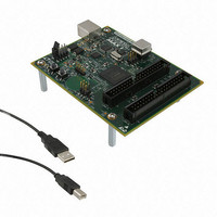
DK-DEV-5M570ZN Altera, DK-DEV-5M570ZN Datasheet - Page 128

DK-DEV-5M570ZN
Manufacturer Part Number
DK-DEV-5M570ZN
Description
KIT DEV MAX V 5M570Z
Manufacturer
Altera
Series
MAX® Vr
Type
CPLDr
Datasheets
1.DK-DEV-5M570ZN.pdf
(30 pages)
2.DK-DEV-5M570ZN.pdf
(2 pages)
3.DK-DEV-5M570ZN.pdf
(30 pages)
4.DK-DEV-5M570ZN.pdf
(164 pages)
5.DK-DEV-5M570ZN.pdf
(24 pages)
Specifications of DK-DEV-5M570ZN
Contents
Board, Cable(s), Software and Documentation
Silicon Manufacturer
Altera
Core Architecture
CPLD
Core Sub-architecture
MAX
Silicon Core Number
5M
Silicon Family Name
MAX V
Kit Contents
MAX V CPLD Development Board, USB Cable
Rohs Compliant
Yes
Lead Free Status / RoHS Status
Lead free / RoHS Compliant
For Use With/related Products
5M570ZF256
Lead Free Status / Rohs Status
Compliant
Other names
544-2722
Available stocks
Company
Part Number
Manufacturer
Quantity
Price
7–26
Figure 7–21. READ Operation Sequence for Extended Mode
MAX V Device Handbook
SCK
nCS
SO
SI
MSB
0
READ
READ is the instruction for data transmission, where the data is read from the UFM
block. When data transfer is taking place, the MSB is always the first bit to be
transmitted or received. The data output stream is continuous through all addresses
until it is terminated by a low-to-high transition at the nCS port. The READ operation is
always performed through the following sequence in SPI, as shown in
1. nCS is pulled low to indicate the start of transmission.
2. An 8-bit READ opcode (00000011) is received from the master device. (If internal
3. A 16-bit address is received from the master device. The LSB of the address is
4. Data is transmitted for as many words as needed by the slave device through SO
5. nCS is pulled back to high to indicate the end of transmission.
For SPI Base mode, the READ operation is always performed through the following
sequence in SPI:
1. nCS is pulled low to indicate the start of transmission.
2. An 8-bit READ opcode (00000011) is received from the master device, followed by
3. Data is transmitted for as many words as needed by the slave device through SO
4. nCS is pulled back to high to indicate the end of transmission.
1
Instruction
2
programming is in progress, READ is ignored and not accepted).
received last. Because the UFM block can take only nine bits of address maximum,
the first seven address bits received are discarded.
for READ operation. When the end of the UFM storage array is reached, the address
counter rolls over to the start of the UFM to continue the READ operation.
an 8-bit address. If internal programming is in progress, the READ operation is
ignored and not accepted.
for READ operation. The internal address pointer automatically increments until the
highest memory address is reached (address 255 only because the UFM sector 0 is
used). The address counter will not roll over when address 255 is reached. The SO
output is set to high-impedance (Z) when all eight data bits from address 255 have
been shifted out through the SO port.
8-bit
03
3
H
4
High Impedance
5 6 7
8
MSB
9 10 11
Address
16-bit
20 21 22 23 24 25 26 27
MSB
16-bit Data Out 1
36 37 38 39
Chapter 7: User Flash Memory in MAX V Devices
MSB
16-bit Data Out 2
January 2011 Altera Corporation
Software Support for UFM Block
Figure
7–21:


