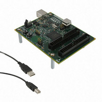
DK-DEV-5M570ZN Altera, DK-DEV-5M570ZN Datasheet - Page 105

DK-DEV-5M570ZN
Manufacturer Part Number
DK-DEV-5M570ZN
Description
KIT DEV MAX V 5M570Z
Manufacturer
Altera
Series
MAX® Vr
Type
CPLDr
Datasheets
1.DK-DEV-5M570ZN.pdf
(30 pages)
2.DK-DEV-5M570ZN.pdf
(2 pages)
3.DK-DEV-5M570ZN.pdf
(30 pages)
4.DK-DEV-5M570ZN.pdf
(164 pages)
5.DK-DEV-5M570ZN.pdf
(24 pages)
Specifications of DK-DEV-5M570ZN
Contents
Board, Cable(s), Software and Documentation
Silicon Manufacturer
Altera
Core Architecture
CPLD
Core Sub-architecture
MAX
Silicon Core Number
5M
Silicon Family Name
MAX V
Kit Contents
MAX V CPLD Development Board, USB Cable
Rohs Compliant
Yes
Lead Free Status / RoHS Status
Lead free / RoHS Compliant
For Use With/related Products
5M570ZF256
Lead Free Status / Rohs Status
Compliant
Other names
544-2722
Available stocks
Company
Part Number
Manufacturer
Quantity
Price
Chapter 7: User Flash Memory in MAX V Devices
UFM Functional Description
UFM Functional Description
Table 7–4. UFM Interface Signals (Part 1 of 2)
January 2011 Altera Corporation
DRDin
DRCLK
DRSHFT
ARDin
ARCLK
ARSHFT
Port Name
Port Type
Input
Input
Input
Input
Input
Input
Figure 7–1
Figure 7–1. UFM Block and Interface Signals
Table 7–4
Serial input to the data register. It is used to enter a data word when writing to the UFM. The
data register is 16 bits wide and data is shifted serially from the LSB to the MSB with each
DRCLK. This port is required for writing, but unused if the UFM is in read-only mode.
Clock input that controls the data register. It is required and takes control when data is
shifted from DRDin to DRDout or loaded in parallel from the flash memory. The maximum
frequency for DRCLK is 10 MHz.
Signal that determines whether to shift the data register or load it on a DRCLK edge. A high
value shifts the data from DRDin into the LSB of the data register and from the MSB of the
data register out to DRDout. A low value loads the value of the current address in the flash
memory to the data register.
Serial input to the address register. It is used to enter the address of a memory location to
read, program, or erase. The address register is 9 bits wide for the UFM size of 8,192 bits.
Clock input that controls the address register. It is required when shifting the address data
from ARDin into the address register or during the increment stage. The maximum
frequency for ARCLK is 10 MHz.
Signal that determines whether to shift the address register or increment it on an ARCLK
edge. A high value shifts the data from ARDin serially into the address register. A low value
increments the current address by 1. The address register rolls over to 0 when the address
space is at the maximum.
lists the MAX V UFM block input and output interface signals.
is the block diagram of the MAX V UFM block and the interface signals.
PROGRAM
OSC_ENA
DRSHFT
ARSHFT
ERASE
DRCLK
ARCLK
DRDin
ARDin
Register
Address
9
UFM Block
Description
16
Data Register
OSC
UFM Sector 1
UFM Sector 0
Program
Control
Erase
16
: _
4
RTP_BUSY
BUSY
OSC
DRDout
MAX V Device Handbook
7–3


