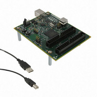
DK-DEV-5M570ZN Altera, DK-DEV-5M570ZN Datasheet - Page 95

DK-DEV-5M570ZN
Manufacturer Part Number
DK-DEV-5M570ZN
Description
KIT DEV MAX V 5M570Z
Manufacturer
Altera
Series
MAX® Vr
Type
CPLDr
Datasheets
1.DK-DEV-5M570ZN.pdf
(30 pages)
2.DK-DEV-5M570ZN.pdf
(2 pages)
3.DK-DEV-5M570ZN.pdf
(30 pages)
4.DK-DEV-5M570ZN.pdf
(164 pages)
5.DK-DEV-5M570ZN.pdf
(24 pages)
Specifications of DK-DEV-5M570ZN
Contents
Board, Cable(s), Software and Documentation
Silicon Manufacturer
Altera
Core Architecture
CPLD
Core Sub-architecture
MAX
Silicon Core Number
5M
Silicon Family Name
MAX V
Kit Contents
MAX V CPLD Development Board, USB Cable
Rohs Compliant
Yes
Lead Free Status / RoHS Status
Lead free / RoHS Compliant
For Use With/related Products
5M570ZF256
Lead Free Status / Rohs Status
Compliant
Other names
544-2722
Available stocks
Company
Part Number
Manufacturer
Quantity
Price
MV51006-1.0
IEEE Std. 1149.1 Boundary-Scan Support
Table 6–1. JTAG Instructions for MAX V Devices (Part 1 of 2)
© 2010 Altera Corporation. All rights reserved. ALTERA, ARRIA, CYCLONE, HARDCOPY, MAX, MEGACORE, NIOS, QUARTUS and STRATIX are Reg. U.S. Pat. & Tm. Off.
and/or trademarks of Altera Corporation in the U.S. and other countries. All other trademarks and service marks are the property of their respective holders as described at
www.altera.com/common/legal.html. Altera warrants performance of its semiconductor products to current specifications in accordance with Altera’s standard warranty, but
reserves the right to make changes to any products and services at any time without notice. Altera assumes no responsibility or liability arising out of the application or use of any
information, product, or service described herein except as expressly agreed to in writing by Altera. Altera customers are advised to obtain the latest version of device
specifications before relying on any published information and before placing orders for products or services.
MAX V Device Handbook
December 2010
December 2010
MV51006-1.0
SAMPLE/PRELOAD
EXTEST
BYPASS
USERCODE
JTAG Instruction
(1)
This chapter describes the IEEE Standard 1149.1 JTAG BST circuitry that is supported
in MAX
multiple devices in a minimum time with the IEEE Standard 1532 in-system
programmability (ISP). This chapter also describes the programming sequence, types
of programming with the Quartus
security.
This chapter includes the following sections:
■
■
All MAX V devices provide JTAG BST circuitry that complies with the
IEEE Std. 1149.1-2001 specification. You can only perform JTAG boundary-scan
testing after you have fully powered the V
amount of configuration time (t
MAX V devices can use the JTAG port with either the Quartus II software or
hardware with Programmer Object File (.pof), Jam
Language (STAPL) Format File (.jam), or Jam Byte Code Files (.jbc).
JTAG pins support 1.5-V, 1.8-V, 2.5-V, and 3.3-V I/O standards. The V
where it is located determines the supported voltage level and standard. The
dedicated JTAG pins reside in Bank 1 of all MAX V devices.
Table 6–1
“IEEE Std. 1149.1 Boundary-Scan Support” on page 6–1
“In-System Programmability” on page 6–5
Instruction Code
®
00 0000 0101
00 0000 1111
11 1111 1111
00 0000 0111
V devices and how you can enable concurrent in-system programming of
lists the JTAG instructions supported in MAX V devices.
6. JTAG and In-System Programmability
Allows you to capture and examine a snapshot of signals at the
device pins if the device is operating in normal mode. Permits an
initial data pattern to be an output at the device pins.
Allows you to test the external circuitry and board-level
interconnects by forcing a test pattern at the output pins and
capturing test results at the input pins.
Places the 1-bit bypass register between the TDI and TDO pins,
which allows the boundary-scan test (BST) data to pass
synchronously through target devices to adjacent devices during
normal device operation.
Selects the 32-bit USERCODE register and places it between the TDI
and TDO pins, allowing you to shift the USERCODE register out of the
TDO pin serially. If you do not specify the USERCODE in the Quartus II
software, the 32-bit USERCODE register defaults to all 1’s.
CONFIG
®
II software or external hardware, and design
) have passed. For in-system programming,
CCINT
and all V
™
Description
Standard Test and Programming
CCIO
in MAX V Devices
banks and a certain
CCIO
of the bank
Subscribe


