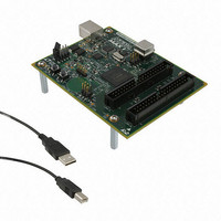
DK-DEV-5M570ZN Altera, DK-DEV-5M570ZN Datasheet - Page 161

DK-DEV-5M570ZN
Manufacturer Part Number
DK-DEV-5M570ZN
Description
KIT DEV MAX V 5M570Z
Manufacturer
Altera
Series
MAX® Vr
Type
CPLDr
Datasheets
1.DK-DEV-5M570ZN.pdf
(30 pages)
2.DK-DEV-5M570ZN.pdf
(2 pages)
3.DK-DEV-5M570ZN.pdf
(30 pages)
4.DK-DEV-5M570ZN.pdf
(164 pages)
5.DK-DEV-5M570ZN.pdf
(24 pages)
Specifications of DK-DEV-5M570ZN
Contents
Board, Cable(s), Software and Documentation
Silicon Manufacturer
Altera
Core Architecture
CPLD
Core Sub-architecture
MAX
Silicon Core Number
5M
Silicon Family Name
MAX V
Kit Contents
MAX V CPLD Development Board, USB Cable
Rohs Compliant
Yes
Lead Free Status / RoHS Status
Lead free / RoHS Compliant
For Use With/related Products
5M570ZF256
Lead Free Status / Rohs Status
Compliant
Other names
544-2722
Available stocks
Company
Part Number
Manufacturer
Quantity
Price
Chapter 8: JTAG Boundary-Scan Testing in MAX V Devices
Disabling IEEE Std. 1149.1 BST Circuitry
Disabling IEEE Std. 1149.1 BST Circuitry
Guidelines for IEEE Std. 1149.1 Boundary-Scan Testing
Boundary-Scan Description Language Support
December 2010 Altera Corporation
1
You can enable the IEEE Std. 1149.1 BST circuitry for MAX V devices after device
powers up. You must enable this circuitry only if you use the BST or ISP features. This
section describes how to disable the IEEE Std. 1149.1 circuitry to ensure that the
circuitry is not inadvertently enabled when it is not required.
Table 8–3
that have dedicated IEEE Std. 1149.1 pins.
Table 8–3. Disabling IEEE Std. 1149.1 Circuitry for MAX V Devices
When performing boundary-scan testing with IEEE Std. 1149.1 devices, use the
following guidelines:
■
■
■
If problems persist, contact
The BSDL—a subset of VHDL—provides a syntax that allows you to describe the
features of an IEEE Std. 1149.1 BST-capable device that can be tested. Test software
development systems then use the BSDL files for test generation, analysis, failure
diagnostics, and in-system programming.
Notes to
(1) There is no software option to disable JTAG in MAX V devices. The JTAG pins are dedicated.
(2) VCC refers to V
(3) The TCK signal may also be tied high. If TCK is tied high, power-up conditions must ensure that TMS is pulled high
If a pattern (for example, a 10-bit 1010101010 pattern) does not shift out of the
instruction register through the TDO pin during the first clock cycle of the SHIFT_IR
state, the proper TAP controller state has not been reached. To solve this problem,
try one of the following procedures:
■
■
Perform a SAMPLE/PRELOAD test cycle before the first EXTEST test cycle to ensure that
known data is present at the device pins when EXTEST mode is entered. If the OEJ
update register contains a 0, the data in the OUTJ update register will be driven out.
The state must be known and correct to avoid contention with other devices in the
system.
Do not perform EXTEST and SAMPLE/PRELOAD tests during ISP. These instructions
are supported before and after ISP but not during ISP.
before TCK. Pulling TCK low avoids this power-up condition.
Verify that the TAP controller has reached the SHIFT_IR state correctly. To
advance the TAP controller to the SHIFT_IR state, return to the RESET state and
clock the code 01100 on the TMS pin.
Check the connections to the VCC, GND, and JTAG pins on the device.
VCC
Table
TMS
lists the pin connections necessary for disabling JTAG in MAX V devices
(2)
8–3:
CCIO
of Bank 1.
Technical
GND
TCK
(3)
JTAG Pins
Support.
(1)
VCC
TDI
(2)
MAX V Device Handbook
Leave Open
TDO
8–15


