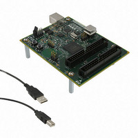
DK-DEV-5M570ZN Altera, DK-DEV-5M570ZN Datasheet - Page 100

DK-DEV-5M570ZN
Manufacturer Part Number
DK-DEV-5M570ZN
Description
KIT DEV MAX V 5M570Z
Manufacturer
Altera
Series
MAX® Vr
Type
CPLDr
Datasheets
1.DK-DEV-5M570ZN.pdf
(30 pages)
2.DK-DEV-5M570ZN.pdf
(2 pages)
3.DK-DEV-5M570ZN.pdf
(30 pages)
4.DK-DEV-5M570ZN.pdf
(164 pages)
5.DK-DEV-5M570ZN.pdf
(24 pages)
Specifications of DK-DEV-5M570ZN
Contents
Board, Cable(s), Software and Documentation
Silicon Manufacturer
Altera
Core Architecture
CPLD
Core Sub-architecture
MAX
Silicon Core Number
5M
Silicon Family Name
MAX V
Kit Contents
MAX V CPLD Development Board, USB Cable
Rohs Compliant
Yes
Lead Free Status / RoHS Status
Lead free / RoHS Compliant
For Use With/related Products
5M570ZF256
Lead Free Status / Rohs Status
Compliant
Other names
544-2722
Available stocks
Company
Part Number
Manufacturer
Quantity
Price
6–6
MAX V Device Handbook
IEEE 1532 Support
Jam Standard Test and Programming Language
Programming Sequence
f
f
The JTAG circuitry and ISP instruction set in MAX V devices are compliant to the
IEEE-1532-2002 programming specification. This provides industry-standard
hardware and software for in-system programming among multiple vendor
programmable logic devices (PLDs) in a JTAG chain.
For more information about MAX V 1532 Boundary-Scan Description Language
(.bsd) files, refer to the
You can use the Jam STAPL to program MAX V devices with in-circuit testers, PCs, or
embedded processors. The Jam byte code is also supported for MAX V devices. These
software programming protocols provide a compact embedded solution for
programming MAX V devices.
For more information, refer to
Device
During in-system programming, 1532 instructions, addresses, and data are shifted
into the MAX V device through the TDI input pin. Data is shifted out through the TDO
output pin and compared with the expected data.
To program a pattern into the device, follow these steps:
1. Enter ISP—The enter ISP stage ensures that the I/O pins transition smoothly from
2. Check ID—The silicon ID is checked before any Program or Verify process. The
3. Sector Erase—Erasing the device in-system involves shifting in the instruction to
4. Program—Programming the device in-system involves shifting in the address,
5. Verify—Verifying a MAX V device in-system involves shifting in addresses,
6. Exit ISP—An exit ISP stage ensures that the I/O pins transition smoothly from ISP
user mode to ISP mode.
time required to read this silicon ID is relatively small compared to the overall
programming time.
erase the device and applying an erase pulse or pulses. The erase pulse is
automatically generated internally by waiting in the run, test, or idle state for the
specified erase pulse time of 500 ms for the CFM block and 500 ms for each sector
of the user flash memory (UFM) block.
data, and program instruction and generating the program pulse to program the
flash cells. The program pulse is automatically generated internally by waiting in
the run/test/idle state for the specified program pulse time of 75 µs. This process
is repeated for each address in the CFM and UFM blocks.
applying the verify instruction to generate the read pulse, and shifting out the data
for comparison. This process is repeated for each CFM and UFM address.
mode to user mode.
Programming.
IEEE 1532 BSDL Files
AN 425: Using Command-Line Jam STAPL Solution for
Chapter 6: JTAG and In-System Programmability in MAX V Devices
page of the Altera website.
December 2010 Altera Corporation
In-System Programmability


