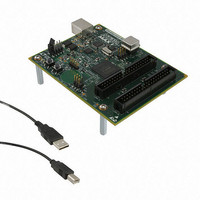
DK-DEV-5M570ZN Altera, DK-DEV-5M570ZN Datasheet - Page 138

DK-DEV-5M570ZN
Manufacturer Part Number
DK-DEV-5M570ZN
Description
KIT DEV MAX V 5M570Z
Manufacturer
Altera
Series
MAX® Vr
Type
CPLDr
Datasheets
1.DK-DEV-5M570ZN.pdf
(30 pages)
2.DK-DEV-5M570ZN.pdf
(2 pages)
3.DK-DEV-5M570ZN.pdf
(30 pages)
4.DK-DEV-5M570ZN.pdf
(164 pages)
5.DK-DEV-5M570ZN.pdf
(24 pages)
Specifications of DK-DEV-5M570ZN
Contents
Board, Cable(s), Software and Documentation
Silicon Manufacturer
Altera
Core Architecture
CPLD
Core Sub-architecture
MAX
Silicon Core Number
5M
Silicon Family Name
MAX V
Kit Contents
MAX V CPLD Development Board, USB Cable
Rohs Compliant
Yes
Lead Free Status / RoHS Status
Lead free / RoHS Compliant
For Use With/related Products
5M570ZF256
Lead Free Status / Rohs Status
Compliant
Other names
544-2722
Available stocks
Company
Part Number
Manufacturer
Quantity
Price
7–36
Table 7–15. Parallel Interface Signals
MAX V Device Handbook
DI[15..0]
DO[15..0]
ADDR[8..0]
nREAD
nWRITE
nERASE
nBUSY
DATA_VALID
Pin
Parallel Interface
16-bit data Input
16-bit data Output
Address Register
READ Instruction Signal
WRITE Instruction Signal
ERASE Instruction Signal
BUSY Signal
Data Valid
This interface allows for parallel communication between the UFM block and outside
logic. After the READ request, WRITE request, or ERASE request is asserted (active low
assertion), the outside logic or device (such as a microcontroller) can continue its
operation while the data in the UFM is retrieved, written, or erased. During this time,
the nBUSY signal is driven “low” to indicate that it is not available to respond to any
further request. After the operation is complete, the nBUSY signal is brought back to
“high” to indicate that it is now available to service a new request. If it was the Read
request, the DATA_VALID is driven “high” to indicate that the data at the DO port is the
valid data from the last read address.
Asserting READ, WRITE, and ERASE at the same time is not allowed. Multiple requests
are ignored and nothing is read from, written to, or erased in the UFM block. There is
no support for sequential read and page write in the parallel interface. For both the
read only and the read/write modes of the parallel interface, OSC_ENA is always
asserted, enabling the internal oscillator.
functions.
Even though the ALTUFM megafunction allows you to select the address widths
range from 3 bits to 9 bits, the UFM block always expects a full 9 bits for the width of
the address register. Therefore, the ALTUFM megafunction will always pad the
remaining LSBs of the address register with '0's if the register width selected is less
than 9 bits. The address register will point to sector 0 if the address received at the
address register starts with a '0'. The address register will point to sector 1 if the
address received starts with a '1'.
Even though you can select an optional data register width of 3 to 16 bits using the
ALTUFM megafunction, the UFM block always expects full 16 bits width for the data
register. Reading from the data register always proceeds from MSB to LSB. The
ALTUFM megafunction always pads the remaining LSBs of the data register with 1s if
the user selects a data width of less than 16-bits.
Description
Receive 16-bit data in parallel. You can select an optional width of 3 to
16 bits using the ALTUFM megafunction.
Transmit 16-bit data in parallel. You can select an optional width of 3 to
16 bits using the ALTUFM megafunction.
Operation sequence refers to the data that is pointed to by the address
register. You can determine the address bus width using the ALTUFM
megafunction.
Initiates a read sequence.
Initiates a write sequence.
Initiates a SECTOR-ERASE sequence indicated by the MSB of the
ADDR[] port.
Driven low to notify that it is not available to respond to any further
request.
Driven high to indicate that the data at the DO port is the valid data from
the last read address for read request.
Table 7–15
Chapter 7: User Flash Memory in MAX V Devices
Function
lists the parallel interface pins and
January 2011 Altera Corporation
Software Support for UFM Block


