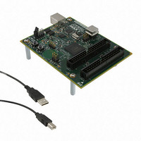
DK-DEV-5M570ZN Altera, DK-DEV-5M570ZN Datasheet - Page 148

DK-DEV-5M570ZN
Manufacturer Part Number
DK-DEV-5M570ZN
Description
KIT DEV MAX V 5M570Z
Manufacturer
Altera
Series
MAX® Vr
Type
CPLDr
Datasheets
1.DK-DEV-5M570ZN.pdf
(30 pages)
2.DK-DEV-5M570ZN.pdf
(2 pages)
3.DK-DEV-5M570ZN.pdf
(30 pages)
4.DK-DEV-5M570ZN.pdf
(164 pages)
5.DK-DEV-5M570ZN.pdf
(24 pages)
Specifications of DK-DEV-5M570ZN
Contents
Board, Cable(s), Software and Documentation
Silicon Manufacturer
Altera
Core Architecture
CPLD
Core Sub-architecture
MAX
Silicon Core Number
5M
Silicon Family Name
MAX V
Kit Contents
MAX V CPLD Development Board, USB Cable
Rohs Compliant
Yes
Lead Free Status / RoHS Status
Lead free / RoHS Compliant
For Use With/related Products
5M570ZF256
Lead Free Status / Rohs Status
Compliant
Other names
544-2722
Available stocks
Company
Part Number
Manufacturer
Quantity
Price
8–2
IEEE Std. 1149.1 BST Architecture
MAX V Device Handbook
■
■
■
In addition to BST, you can use the IEEE Std. 1149.1 controller for in-system
programming for MAX V devices. MAX V devices support IEEE 1532 programming,
which uses the IEEE Std. 1149.1 test access port (TAP) interface. However, this chapter
only describes the BST feature of the IEEE Std. 1149.1 circuitry.
A MAX V device operating in IEEE Std. 1149.1 BST mode uses four required pins, TDI,
TDO, TMS, and TCK.
Table 8–1
pin.
Table 8–1. IEEE Std. 1149.1 Pin Descriptions
The IEEE Std. 1149.1 BST circuitry requires the following registers:
■
■
■
TDI
TDO
TMS
TCK
Notes to
(1) The TDI and TMS pins have internal weak pull-up resistors
(2) The TCK pin has an internal weak pull-down resistor
Pin
“Disabling IEEE Std. 1149.1 BST Circuitry” on page 8–15
“Guidelines for IEEE Std. 1149.1 Boundary-Scan Testing” on page 8–15
“Boundary-Scan Description Language Support” on page 8–15
The instruction register determines which action to perform and which data
register to access.
The bypass register (which is a 1-bit long data register) provides a
minimum-length serial path between the TDI and TDO pins.
The boundary-scan register that is a shift register composed of all the BSCs of the
device.
(1)
(2)
(1)
Table
lists the functions of each of these pins. MAX V devices do not have a TRST
Test mode select
8–1:
Test data output
Test clock input
Test data input
Description
Serial input pin for instructions as well as test and
programming data. Data is shifted in on the rising edge of TCK.
Serial data output pin for instructions as well as test and
programming data. Data is shifted out on the falling edge of
TCK. The pin is tri-stated if data is not being shifted out of the
device.
Input pin that provides the control signal to determine the
transitions of the TAP controller state machine. Transitions
within the state machine occur at the rising edge of TCK.
Therefore, you must set up the TMS before the rising edge of
TCK. TMS is evaluated on the rising edge of TCK.
The clock input to the BST circuitry. Some operations occur at
the rising edge, while others occur at the falling edge.
Chapter 8: JTAG Boundary-Scan Testing in MAX V Devices
Function
December 2010 Altera Corporation
IEEE Std. 1149.1 BST Architecture


