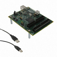
DK-DEV-5M570ZN Altera, DK-DEV-5M570ZN Datasheet - Page 84

DK-DEV-5M570ZN
Manufacturer Part Number
DK-DEV-5M570ZN
Description
KIT DEV MAX V 5M570Z
Manufacturer
Altera
Series
MAX® Vr
Type
CPLDr
Datasheets
1.DK-DEV-5M570ZN.pdf
(30 pages)
2.DK-DEV-5M570ZN.pdf
(2 pages)
3.DK-DEV-5M570ZN.pdf
(30 pages)
4.DK-DEV-5M570ZN.pdf
(164 pages)
5.DK-DEV-5M570ZN.pdf
(24 pages)
Specifications of DK-DEV-5M570ZN
Contents
Board, Cable(s), Software and Documentation
Silicon Manufacturer
Altera
Core Architecture
CPLD
Core Sub-architecture
MAX
Silicon Core Number
5M
Silicon Family Name
MAX V
Kit Contents
MAX V CPLD Development Board, USB Cable
Rohs Compliant
Yes
Lead Free Status / RoHS Status
Lead free / RoHS Compliant
For Use With/related Products
5M570ZF256
Lead Free Status / Rohs Status
Compliant
Other names
544-2722
Available stocks
Company
Part Number
Manufacturer
Quantity
Price
- DK-DEV-5M570ZN PDF datasheet
- DK-DEV-5M570ZN PDF datasheet #2
- DK-DEV-5M570ZN PDF datasheet #3
- DK-DEV-5M570ZN PDF datasheet #4
- DK-DEV-5M570ZN PDF datasheet #5
- Current page: 84 of 164
- Download datasheet (5Mb)
4–4
Figure 4–2. Transistor-Level I/O Buffers for MAX V Devices
Figure 4–3. ESD Protection During Positive Voltage Zap
MAX V Device Handbook
Figure 4–2
This design ensures that the output buffers do not drive when V
before V
sudden voltage spikes during hot insertion. The V
3.3-V tolerant circuit capacitance.
The CMOS output drivers in the I/O pins intrinsically provide electrostatic discharge
(ESD) protection. There are two cases to consider for ESD voltage strikes—positive
voltage zap and negative voltage zap.
A positive ESD voltage zap occurs when a positive voltage is present on an I/O pin
due to an ESD charge event. This can cause the N+ (Drain)/ P-Substrate junction of
the N-channel drain to break down and the N+ (Drain)/P-Substrate/N+ (Source)
intrinsic bipolar transistor turn on to discharge ESD current from I/O pin to GND.
The dashed line in
ESD zap.
n+
IOE Signal
p - well
CCINT
shows a transistor-level cross section of the MAX V device I/O buffers.
I/O
or if the I/O pad voltage is higher than V
n+
Figure 4–3
GND
VPAD
Source
Drain
Drain
Source
PMOS
NMOS
shows the ESD current discharge path during a positive
Larger of VCCIO or VPAD
p+
IOE Signal or the
Gate
Gate
Chapter 4: Hot Socketing and Power-On Reset in MAX V Devices
n - well
P-Substrate
VCCIO
p+
Hot-Socketing Feature Implementation in MAX V Devices
p - substrate
N+
N+
VCCIO or VPAD
The Larger of
PAD
D
S
n+
GND
I/O
G
leakage current charges the
CCIO
. This also applies for
December 2010 Altera Corporation
Ensures 3.3-V
Tolerance and
Hot-Socket
Protection
CCIO
is powered
Related parts for DK-DEV-5M570ZN
Image
Part Number
Description
Manufacturer
Datasheet
Request
R

Part Number:
Description:
KIT DEV ARRIA II GX FPGA 2AGX125
Manufacturer:
Altera
Datasheet:

Part Number:
Description:
KIT DEV CYCLONE III LS EP3CLS200
Manufacturer:
Altera
Datasheet:

Part Number:
Description:
KIT DEV STRATIX IV FPGA 4SE530
Manufacturer:
Altera
Datasheet:

Part Number:
Description:
KIT DEV FPGA 2AGX260 W/6.375G TX
Manufacturer:
Altera
Datasheet:

Part Number:
Description:
KIT DEV STRATIX V FPGA 5SGXEA7
Manufacturer:
Altera
Datasheet:

Part Number:
Description:
KIT DEVELOPMENT STRATIX III
Manufacturer:
Altera
Datasheet:

Part Number:
Description:
KIT DEVELOPMENT STRATIX IV
Manufacturer:
Altera
Datasheet:

Part Number:
Description:
KIT DEV ARRIA GX 1AGX60N
Manufacturer:
Altera
Datasheet:

Part Number:
Description:
KIT STARTER CYCLONE IV GX
Manufacturer:
Altera
Datasheet:

Part Number:
Description:
KIT DEVELOPMENT STRATIX IV
Manufacturer:
Altera
Datasheet:

Part Number:
Description:
CPLD, EP610 Family, ECMOS Process, 300 Gates, 16 Macro Cells, 16 Reg., 16 User I/Os, 5V Supply, 35 Speed Grade, 24DIP
Manufacturer:
Altera Corporation
Datasheet:

Part Number:
Description:
CPLD, EP610 Family, ECMOS Process, 300 Gates, 16 Macro Cells, 16 Reg., 16 User I/Os, 5V Supply, 15 Speed Grade, 24DIP
Manufacturer:
Altera Corporation
Datasheet:


