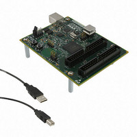
DK-DEV-5M570ZN Altera, DK-DEV-5M570ZN Datasheet - Page 129

DK-DEV-5M570ZN
Manufacturer Part Number
DK-DEV-5M570ZN
Description
KIT DEV MAX V 5M570Z
Manufacturer
Altera
Series
MAX® Vr
Type
CPLDr
Datasheets
1.DK-DEV-5M570ZN.pdf
(30 pages)
2.DK-DEV-5M570ZN.pdf
(2 pages)
3.DK-DEV-5M570ZN.pdf
(30 pages)
4.DK-DEV-5M570ZN.pdf
(164 pages)
5.DK-DEV-5M570ZN.pdf
(24 pages)
Specifications of DK-DEV-5M570ZN
Contents
Board, Cable(s), Software and Documentation
Silicon Manufacturer
Altera
Core Architecture
CPLD
Core Sub-architecture
MAX
Silicon Core Number
5M
Silicon Family Name
MAX V
Kit Contents
MAX V CPLD Development Board, USB Cable
Rohs Compliant
Yes
Lead Free Status / RoHS Status
Lead free / RoHS Compliant
For Use With/related Products
5M570ZF256
Lead Free Status / Rohs Status
Compliant
Other names
544-2722
Available stocks
Company
Part Number
Manufacturer
Quantity
Price
Chapter 7: User Flash Memory in MAX V Devices
Software Support for UFM Block
Figure 7–22. READ Operation for Base Mode
January 2011 Altera Corporation
SCK
nCS
SO
SI
MSB
1
Figure 7–22
WRITE
WRITE is the instruction for data transmission, where the data is written to the UFM
block. The targeted location in the UFM block that will be written must be in the
erased state (FFFFH) before initiating a WRITE operation. When data transfer is taking
place, the MSB is always the first bit to be transmitted or received. nCS must be driven
high before the instruction is executed internally. You may poll the nRDY bit in the
software status register for the completion of the internal self-timed WRITE cycle. For
SPI Extended mode, the WRITE operation is always done through the following
sequence, as shown in
1. nCS is pulled low to indicate the start of transmission.
2. An 8-bit WRITE opcode (00000010) is received from the master device. If internal
3. A 16-bit address is received from the master device. The LSB of the address will be
4. A check is carried out on the status register (see
5. One word (16 bits) of data is transmitted to the slave device through SI.
6. nCS is pulled back to high to indicate the end of transmission.
For SPI Base mode, the WRITE operation is always performed through the following
sequence in SPI:
1. nCS is pulled low to indicate the start of transmission.
2. An 8-bit WRITE opcode (00000010) is received. If the internal programming is in
3. An 8-bit address is received. A check is carried out on the status register (see
2 3
Instruction
programming is in progress, the WRITE operation is ignored and not accepted.
received last. Because the UFM block can take only nine bits of address maximum,
the first seven address bits received are discarded.
WRITE operation has been enabled, and the address is outside of the protected
region; otherwise, Step 5 is bypassed.
progress, the WRITE operation is ignored and not accepted.
Table
is outside of the protected region; otherwise, Step 4 is skipped.
8-bit
03
4
H
High Impedance
5
6
7–11) to determine if the WRITE operation has been enabled, and the address
7 8 9 10 11 12 13 14 15 16 17 18 19
shows the READ operation sequence for Base mode.
MSB
Address
8-bit
Figure
MSB
8-bit Data Out 1
7–23:
20 21 22 23 23
MSB
8-bit Data Out 2
Table
7–11) to determine if the
MAX V Device Handbook
7–27


