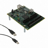
DK-DEV-5M570ZN Altera, DK-DEV-5M570ZN Datasheet - Page 18

DK-DEV-5M570ZN
Manufacturer Part Number
DK-DEV-5M570ZN
Description
KIT DEV MAX V 5M570Z
Manufacturer
Altera
Series
MAX® Vr
Type
CPLDr
Datasheets
1.DK-DEV-5M570ZN.pdf
(30 pages)
2.DK-DEV-5M570ZN.pdf
(2 pages)
3.DK-DEV-5M570ZN.pdf
(30 pages)
4.DK-DEV-5M570ZN.pdf
(164 pages)
5.DK-DEV-5M570ZN.pdf
(24 pages)
Specifications of DK-DEV-5M570ZN
Contents
Board, Cable(s), Software and Documentation
Silicon Manufacturer
Altera
Core Architecture
CPLD
Core Sub-architecture
MAX
Silicon Core Number
5M
Silicon Family Name
MAX V
Kit Contents
MAX V CPLD Development Board, USB Cable
Rohs Compliant
Yes
Lead Free Status / RoHS Status
Lead free / RoHS Compliant
For Use With/related Products
5M570ZF256
Lead Free Status / Rohs Status
Compliant
Other names
544-2722
Available stocks
Company
Part Number
Manufacturer
Quantity
Price
2–6
MAX V Device Handbook
LAB Interconnects
LAB Control Signals
Column and row interconnects and LE outputs within the same LAB drive the LAB
local interconnect. Adjacent LABs, from the left and right, can also drive an LAB’s
local interconnect through the DirectLink connection. The DirectLink connection
feature minimizes the use of row and column interconnects, providing higher
performance and flexibility. Each LE can drive 30 other LEs through fast local and
DirectLink interconnects.
Figure 2–4. DirectLink Connection
Each LAB contains dedicated logic for driving control signals to its LEs. The control
signals include two clocks, two clock enables, two asynchronous clears, a
synchronous clear, an asynchronous preset/load, a synchronous load, and
add/subtract control signals, providing a maximum of 10 control signals at a time.
Synchronous load and clear signals are generally used when implementing counters
but they can also be used with other functions.
Each LAB can use two clocks and two clock enable signals. Each LAB’s clock and
clock enable signals are linked. For example, any LE in a particular LAB using the
labclk1 signal also uses labclkena1. If the LAB uses both the rising and falling edges
of a clock, it also uses both LAB-wide clock signals. Deasserting the clock enable
signal turns off the LAB-wide clock.
Each LAB can use two asynchronous clear signals and an asynchronous load/preset
signal. By default, the Quartus II software uses a NOT gate push-back technique to
achieve preset. If you disable the NOT gate push-back option or assign a given register
to power-up high using the Quartus II software, the preset is then achieved using the
asynchronous load signal with asynchronous load data input tied high.
DirectLink interconnect from
left LAB or IOE output
interconnect
DirectLink
to left
Interconnect
Figure 2–4
Local
Logic Element
shows the DirectLink connection.
LE0
LE1
LE2
LE3
LE4
LE5
LE6
LE7
LE8
LE9
LAB
December 2010 Altera Corporation
DirectLink
interconnect
to right
DirectLink interconnect from
right LAB or IOE output
Chapter 2: MAX V Architecture
Logic Array Blocks


