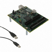
DK-DEV-5M570ZN Altera, DK-DEV-5M570ZN Datasheet - Page 45

DK-DEV-5M570ZN
Manufacturer Part Number
DK-DEV-5M570ZN
Description
KIT DEV MAX V 5M570Z
Manufacturer
Altera
Series
MAX® Vr
Type
CPLDr
Datasheets
1.DK-DEV-5M570ZN.pdf
(30 pages)
2.DK-DEV-5M570ZN.pdf
(2 pages)
3.DK-DEV-5M570ZN.pdf
(30 pages)
4.DK-DEV-5M570ZN.pdf
(164 pages)
5.DK-DEV-5M570ZN.pdf
(24 pages)
Specifications of DK-DEV-5M570ZN
Contents
Board, Cable(s), Software and Documentation
Silicon Manufacturer
Altera
Core Architecture
CPLD
Core Sub-architecture
MAX
Silicon Core Number
5M
Silicon Family Name
MAX V
Kit Contents
MAX V CPLD Development Board, USB Cable
Rohs Compliant
Yes
Lead Free Status / RoHS Status
Lead free / RoHS Compliant
For Use With/related Products
5M570ZF256
Lead Free Status / Rohs Status
Compliant
Other names
544-2722
Available stocks
Company
Part Number
Manufacturer
Quantity
Price
Chapter 2: MAX V Architecture
I/O Structure
December 2010 Altera Corporation
Output Enable Signals
Programmable Drive Strength
1
Each MAX V IOE output buffer supports output enable signals for tri-state control.
The output enable signal can originate from the GCLK[3..0] global signals or from the
MultiTrack interconnect. The MultiTrack interconnect routes output enable signals
and allows for a unique output enable for each output or bidirectional pin.
MAX V devices also provide a chip-wide output enable pin (DEV_OE) to control the
output enable for every output pin in the design. An option set before compilation in
the Quartus II software controls this pin. This chip-wide output enable uses its own
routing resources and does not use any of the four global resources. If this option is
turned on, all outputs on the chip operate normally when DEV_OE is asserted. When
the pin is deasserted, all outputs are tri-stated. If this option is turned off, the DEV_OE
pin is disabled when the device operates in user mode and is available as a user I/O
pin.
The output buffer for each MAX V device I/O pin has two levels of programmable
drive strength control for each of the LVTTL and LVCMOS I/O standards.
Programmable drive strength provides system noise reduction control for high
performance I/O designs. Although a separate slew-rate control feature exists, using
the lower drive strength setting provides signal slew-rate control to reduce system
noise and signal overshoot without the large delay adder associated with the
slew-rate control feature.
with drive strength control. The Quartus II software uses the maximum current
strength as the default setting. The PCI I/O standard is always set at 20 mA with no
alternate setting.
Table 2–7. Programmable Drive Strength
The programmable drive strength feature can be used simultaneously with the
slew-rate control feature.
3.3-V LVTTL
3.3-V LVCMOS
2.5-V LVTTL/LVCMOS
1.8-V LVTTL/LVCMOS
1.5-V LVCMOS
1.2-V LVCMOS
Note to
(1) The I
minimum is specified by the I/O standard. The I
V
the I
OUT
I/O Standard
Table
OH
OH
= V
condition is V
current strength numbers shown are for a condition of a V
OL
2–7:
maximum, where the V
OUT
= 1.7 V and the I
Table 2–7
OL
maximum is specified by the I/O standard. For 2.5-V LVTTL/LVCMOS,
OL
lists the possible settings for the I/O standards
condition is V
IOH/IOL Current Strength Setting (mA)
(Note 1)
OL
current strength numbers shown are for a condition of a
OUT
= 0.7 V.
OUT
16
14
8
8
4
7
6
3
4
2
3
= V
OH
minimum, where the V
MAX V Device Handbook
OH
2–33


