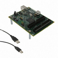
DK-DEV-5M570ZN Altera, DK-DEV-5M570ZN Datasheet - Page 102

DK-DEV-5M570ZN
Manufacturer Part Number
DK-DEV-5M570ZN
Description
KIT DEV MAX V 5M570Z
Manufacturer
Altera
Series
MAX® Vr
Type
CPLDr
Datasheets
1.DK-DEV-5M570ZN.pdf
(30 pages)
2.DK-DEV-5M570ZN.pdf
(2 pages)
3.DK-DEV-5M570ZN.pdf
(30 pages)
4.DK-DEV-5M570ZN.pdf
(164 pages)
5.DK-DEV-5M570ZN.pdf
(24 pages)
Specifications of DK-DEV-5M570ZN
Contents
Board, Cable(s), Software and Documentation
Silicon Manufacturer
Altera
Core Architecture
CPLD
Core Sub-architecture
MAX
Silicon Core Number
5M
Silicon Family Name
MAX V
Kit Contents
MAX V CPLD Development Board, USB Cable
Rohs Compliant
Yes
Lead Free Status / RoHS Status
Lead free / RoHS Compliant
For Use With/related Products
5M570ZF256
Lead Free Status / Rohs Status
Compliant
Other names
544-2722
Available stocks
Company
Part Number
Manufacturer
Quantity
Price
6–8
Document Revision History
Table 6–5. Document Revision History
MAX V Device Handbook
December 2010
Date
Real-Time ISP
Design Security
Programming with External Hardware
f
Version
behavior during the ISP sequence. The in-system programming clamp instruction
allows the device to sample and sustain the value on an output pin (an input pin
remains tri-stated if sampled) or to set a logic high, logic low, or tri-state value
explicitly on any pin. Setting these options is controlled on an individual pin basis
with the Quartus II software.
For more information, refer to
For systems that require more than the DC logic level control of I/O pins, the
real-time ISP feature allows you to update the CFM block with a new design image,
while the current design continues to operate in the SRAM logic array and I/O pins.
A new programming file is updated into the MAX V device without halting the
original operation of your design, saving down-time costs for remote or field
upgrades. The updated CFM block configures the new design into the SRAM after the
next power cycle. You can execute an immediate SRAM configuration without a
power cycle with a specific sequence of ISP commands. The SRAM configuration
without a power cycle takes a specific amount of time (t
I/O pins are tri-stated and weakly pulled-up to V
All MAX V devices contain a programmable security bit that controls access to the
data programmed into the CFM block. If this bit is programmed, you cannot copy or
retrieve the design programming information stored in the CFM block. This feature
provides a high-level design security because programmed data within flash memory
cells is invisible. You can only reset the security bit that controls this function and
other programmed data if the device is erased. The SRAM is also invisible and cannot
be accessed regardless of the security bit setting. The security bit does not protect the
UFM block data, and the UFM is accessible through JTAG or logic array connections.
You can program MAX V devices by downloading the information through in-circuit
testers, embedded processors, the Altera
ByteBlaster™ II, EthernetBlaster, and USB-Blaster cables.
BP Microsystems, System General, and other programming hardware manufacturers
provide programming support for Altera devices. For device support information,
refer to their websites.
Table 6–5
1.0
Initial release.
lists the revision history for this document.
AN 630: Real-Time ISP and ISP Clamp for Altera
Chapter 6: JTAG and In-System Programmability in MAX V Devices
®
ByteblasterMV™, MasterBlaster™,
Changes
CCIO
.
CONFIG
December 2010 Altera Corporation
). During this time, the
Document Revision History
CPLDs.


