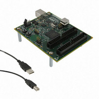
DK-DEV-5M570ZN Altera, DK-DEV-5M570ZN Datasheet - Page 153

DK-DEV-5M570ZN
Manufacturer Part Number
DK-DEV-5M570ZN
Description
KIT DEV MAX V 5M570Z
Manufacturer
Altera
Series
MAX® Vr
Type
CPLDr
Datasheets
1.DK-DEV-5M570ZN.pdf
(30 pages)
2.DK-DEV-5M570ZN.pdf
(2 pages)
3.DK-DEV-5M570ZN.pdf
(30 pages)
4.DK-DEV-5M570ZN.pdf
(164 pages)
5.DK-DEV-5M570ZN.pdf
(24 pages)
Specifications of DK-DEV-5M570ZN
Contents
Board, Cable(s), Software and Documentation
Silicon Manufacturer
Altera
Core Architecture
CPLD
Core Sub-architecture
MAX
Silicon Core Number
5M
Silicon Family Name
MAX V
Kit Contents
MAX V CPLD Development Board, USB Cable
Rohs Compliant
Yes
Lead Free Status / RoHS Status
Lead free / RoHS Compliant
For Use With/related Products
5M570ZF256
Lead Free Status / Rohs Status
Compliant
Other names
544-2722
Available stocks
Company
Part Number
Manufacturer
Quantity
Price
- DK-DEV-5M570ZN PDF datasheet
- DK-DEV-5M570ZN PDF datasheet #2
- DK-DEV-5M570ZN PDF datasheet #3
- DK-DEV-5M570ZN PDF datasheet #4
- DK-DEV-5M570ZN PDF datasheet #5
- Current page: 153 of 164
- Download datasheet (5Mb)
Chapter 8: JTAG Boundary-Scan Testing in MAX V Devices
IEEE Std. 1149.1 BST Operation Control
Figure 8–7. Selecting the Instruction Mode
December 2010 Altera Corporation
TAP_STATE
TMS
TDO
TCK
TDI
TEST_LOGIC/RESET
When the TAP controller is in the TEST_LOGIC/RESET state, the BST circuitry is
disabled, the device is in normal operation, and the instruction register is initialized
with IDCODE as the initial instruction. During device power up, the TAP controller
starts in this TEST_LOGIC/RESET state. In addition, the TAP controller may be forced to
the TEST_LOGIC/RESET state by holding TMS high for five TCK clock cycles. After the
TEST_LOGIC/RESET state, the TAP controller remains in this state as long as TMS
continues to be held high while TCK is clocked.
Figure 8–6
Figure 8–6. IEEE Std. 1149.1 Timing Waveforms
To start the IEEE Std. 1149.1 operation, select an instruction mode by advancing the
TAP controller to the shift instruction register (SHIFT_IR) state and shift in the
appropriate instruction code on the TDI pin.
Figure 8–7
the RESET state, TMS is clocked with the pattern 01100 to advance the TAP controller to
SHIFT_IR state.
Note to
(1) For timing parameter values, refer to the
RUN_TEST/IDLE
Figure 8–6
Captured
Driven
Signal
Signal
shows the timing requirements for the IEEE Std. 1149.1 signals.
shows the entry of the instruction code into the instruction register. From
to Be
to Be
SELECT_DR_SCAN
TMS
TDO
TCK
TDI
:
SELECT_IR_SCAN
t
JCH
t
t
JSZX
JPZX
t
JCP
t
JSSU
t
JCL
CAPTURE_IR
DC and Switching Characteristics for MAX V Devices
t
JSH
SHIFT_IR
t
t
JPCO
JSCO
t
JPSU
(Note 1)
t
JSXZ
t
JPH
t
JPXZ
EXIT1_IR
MAX V Device Handbook
chapter.
8–7
Related parts for DK-DEV-5M570ZN
Image
Part Number
Description
Manufacturer
Datasheet
Request
R

Part Number:
Description:
KIT DEV ARRIA II GX FPGA 2AGX125
Manufacturer:
Altera
Datasheet:

Part Number:
Description:
KIT DEV CYCLONE III LS EP3CLS200
Manufacturer:
Altera
Datasheet:

Part Number:
Description:
KIT DEV STRATIX IV FPGA 4SE530
Manufacturer:
Altera
Datasheet:

Part Number:
Description:
KIT DEV FPGA 2AGX260 W/6.375G TX
Manufacturer:
Altera
Datasheet:

Part Number:
Description:
KIT DEV STRATIX V FPGA 5SGXEA7
Manufacturer:
Altera
Datasheet:

Part Number:
Description:
KIT DEVELOPMENT STRATIX III
Manufacturer:
Altera
Datasheet:

Part Number:
Description:
KIT DEVELOPMENT STRATIX IV
Manufacturer:
Altera
Datasheet:

Part Number:
Description:
KIT DEV ARRIA GX 1AGX60N
Manufacturer:
Altera
Datasheet:

Part Number:
Description:
KIT STARTER CYCLONE IV GX
Manufacturer:
Altera
Datasheet:

Part Number:
Description:
KIT DEVELOPMENT STRATIX IV
Manufacturer:
Altera
Datasheet:

Part Number:
Description:
CPLD, EP610 Family, ECMOS Process, 300 Gates, 16 Macro Cells, 16 Reg., 16 User I/Os, 5V Supply, 35 Speed Grade, 24DIP
Manufacturer:
Altera Corporation
Datasheet:

Part Number:
Description:
CPLD, EP610 Family, ECMOS Process, 300 Gates, 16 Macro Cells, 16 Reg., 16 User I/Os, 5V Supply, 15 Speed Grade, 24DIP
Manufacturer:
Altera Corporation
Datasheet:


