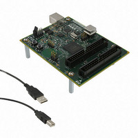
DK-DEV-5M570ZN Altera, DK-DEV-5M570ZN Datasheet - Page 43

DK-DEV-5M570ZN
Manufacturer Part Number
DK-DEV-5M570ZN
Description
KIT DEV MAX V 5M570Z
Manufacturer
Altera
Series
MAX® Vr
Type
CPLDr
Datasheets
1.DK-DEV-5M570ZN.pdf
(30 pages)
2.DK-DEV-5M570ZN.pdf
(2 pages)
3.DK-DEV-5M570ZN.pdf
(30 pages)
4.DK-DEV-5M570ZN.pdf
(164 pages)
5.DK-DEV-5M570ZN.pdf
(24 pages)
Specifications of DK-DEV-5M570ZN
Contents
Board, Cable(s), Software and Documentation
Silicon Manufacturer
Altera
Core Architecture
CPLD
Core Sub-architecture
MAX
Silicon Core Number
5M
Silicon Family Name
MAX V
Kit Contents
MAX V CPLD Development Board, USB Cable
Rohs Compliant
Yes
Lead Free Status / RoHS Status
Lead free / RoHS Compliant
For Use With/related Products
5M570ZF256
Lead Free Status / Rohs Status
Compliant
Other names
544-2722
Available stocks
Company
Part Number
Manufacturer
Quantity
Price
Chapter 2: MAX V Architecture
I/O Structure
December 2010 Altera Corporation
The 5M1270Z and 5M2210Z devices support four I/O banks, as shown in
Each of these banks support all of the LVTTL, LVCMOS, LVDS, and RSDS standards
shown in
PCI clamping diode on inputs and PCI drive compliance on outputs. You must use
Bank 3 for designs requiring PCI compliant I/O pins. The Quartus II software
automatically places I/O pins in this bank if assigned with the PCI I/O standard.
Figure 2–23. I/O Banks for 5M1270Z and 5M2210Z Devices
Notes to
(1)
(2)
(3) This I/O standard is not supported in Bank 1.
(4) Emulated LVDS output using a three resistor network (LVDS_E_3R).
(5) Emulated RSDS output using a three resistor network (RSDS_E_3R).
Each I/O bank has dedicated V
in that bank. A single device can support 1.2-V, 1.5-V, 1.8-V, 2.5-V, and 3.3-V interfaces;
each individual bank can support a different standard. Each I/O bank can support
multiple standards with the same V
V
both the input and output buffers in MAX V devices.
The JTAG pins for MAX V devices are dedicated pins that cannot be used as regular
I/O pins. The pins TMS, TDI, TDO, and TCK support all the I/O standards shown in
Table 2–4 on page 2–29
for all MAX V devices and their I/O standard support is controlled by the V
setting for Bank 1.
CCIO
Figure 2–23
Figure 2–23
I/O Bank 1
is 3.3 V, Bank 3 can support LVTTL, LVCMOS, and 3.3-V PCI. V
Figure
Table
2–23:
is a top view of the silicon die.
is a graphical representation only. Refer to the pin list and the Quartus II software for exact pin locations.
2–4. PCI compliant I/O is supported in Bank 3. Bank 3 supports the
except for PCI and 1.2-V LVCMOS. These pins reside in Bank 1
CCIO
All I/O Banks Support
3.3-V LVTTL/LVCMOS,
2.5-V LVTTL/LVCMOS,
1.8-V LVTTL/LVCMOS,
1.5-V LVCMOS,
1.2-V LVCMOS (3),
LVDS (4),
RSDS(5)
CCIO
pins that determine the voltage standard support
I/O Bank 2
I/O Bank 4
for input and output pins. For example, when
(Note
1),
(2)
MAX V Device Handbook
I/O Bank 3
CCIO
Also Supports
the 3.3-V PCI
I/O Standard
Figure
powers
CCIO
2–23.
2–31


