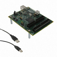
DK-DEV-5M570ZN Altera, DK-DEV-5M570ZN Datasheet - Page 44

DK-DEV-5M570ZN
Manufacturer Part Number
DK-DEV-5M570ZN
Description
KIT DEV MAX V 5M570Z
Manufacturer
Altera
Series
MAX® Vr
Type
CPLDr
Datasheets
1.DK-DEV-5M570ZN.pdf
(30 pages)
2.DK-DEV-5M570ZN.pdf
(2 pages)
3.DK-DEV-5M570ZN.pdf
(30 pages)
4.DK-DEV-5M570ZN.pdf
(164 pages)
5.DK-DEV-5M570ZN.pdf
(24 pages)
Specifications of DK-DEV-5M570ZN
Contents
Board, Cable(s), Software and Documentation
Silicon Manufacturer
Altera
Core Architecture
CPLD
Core Sub-architecture
MAX
Silicon Core Number
5M
Silicon Family Name
MAX V
Kit Contents
MAX V CPLD Development Board, USB Cable
Rohs Compliant
Yes
Lead Free Status / RoHS Status
Lead free / RoHS Compliant
For Use With/related Products
5M570ZF256
Lead Free Status / Rohs Status
Compliant
Other names
544-2722
Available stocks
Company
Part Number
Manufacturer
Quantity
Price
2–32
Table 2–6. LVDS and RSDS Channels supported in MAX V Devices
MAX V Device Handbook
5M40Z
5M80Z
5M160Z
5M240Z
5M570Z
5M1270Z
5M2210Z
Note to
(1) eTx = emulated LVDS output buffers (LVDS_E_3R) or emulated RSDS output buffers (RSDS_E_3R).
Device
Table
Schmitt Trigger
2–6:
64 MBGA
1
10 eTx
10 eTx
—
—
—
—
—
PCI Compliance
The MAX V 5M1270Z and 5M2210Z devices are compliant with PCI applications as
well as all 3.3-V electrical specifications in the PCI Local Bus Specification Revision 2.2.
These devices are also large enough to support PCI intellectual property (IP) cores.
Table 2–5
specifications.
Table 2–5. 3.3-V PCI Electrical Specifications and PCI Timing Support for MAX V Devices
LVDS and RSDS Channels
The MAX V device supports emulated LVDS and RSDS outputs on both row and
column I/O banks. You can configure the rows and columns as emulated LVDS or
RSDS output buffers that use two single-ended output buffers with three external
resistor networks.
The input buffer for each MAX V device I/O pin has an optional Schmitt trigger
setting for the 3.3-V and 2.5-V standards. The Schmitt trigger allows input buffers to
respond to slow input edge rates with a fast output edge rate. Most importantly,
Schmitt triggers provide hysteresis on the input buffer, preventing slow-rising noisy
input signals from ringing or oscillating on the input signal driven into the logic array.
This provides system noise tolerance on MAX V inputs, but adds a small, nominal
input delay.
The JTAG input pins (TMS, TCK, and TDI) have Schmitt trigger buffers that are always
enabled.
The TCK input is susceptible to high pulse glitches when the input signal fall time is
greater than 200 ns for all I/O standards.
64 EQFP
20 eTx
20 eTx
20 eTx
—
—
—
—
shows the MAX V device speed grades that meet the PCI timing
68 MBGA
5M1270Z
5M2210Z
20 eTx
20 eTx
20 eTx
Device
—
—
—
—
100 TQFP
33 eTx
33 eTx
33 eTx
28 eTx
—
—
—
(Note 1)
100 MBGA
33 eTx
33 eTx
28 eTx
—
—
—
—
144 TQFP
49 eTx
49 eTx
42 eTx
—
—
—
—
All Speed Grades
All Speed Grades
33-MHz PCI
December 2010 Altera Corporation
Chapter 2: MAX V Architecture
256 FBGA
75 eTx
90 eTx
83 eTx
—
—
—
—
324 FBGA
115 eTx
115 eTx
I/O Structure
—
—
—
—
—


