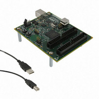
DK-DEV-5M570ZN Altera, DK-DEV-5M570ZN Datasheet - Page 47

DK-DEV-5M570ZN
Manufacturer Part Number
DK-DEV-5M570ZN
Description
KIT DEV MAX V 5M570Z
Manufacturer
Altera
Series
MAX® Vr
Type
CPLDr
Datasheets
1.DK-DEV-5M570ZN.pdf
(30 pages)
2.DK-DEV-5M570ZN.pdf
(2 pages)
3.DK-DEV-5M570ZN.pdf
(30 pages)
4.DK-DEV-5M570ZN.pdf
(164 pages)
5.DK-DEV-5M570ZN.pdf
(24 pages)
Specifications of DK-DEV-5M570ZN
Contents
Board, Cable(s), Software and Documentation
Silicon Manufacturer
Altera
Core Architecture
CPLD
Core Sub-architecture
MAX
Silicon Core Number
5M
Silicon Family Name
MAX V
Kit Contents
MAX V CPLD Development Board, USB Cable
Rohs Compliant
Yes
Lead Free Status / RoHS Status
Lead free / RoHS Compliant
For Use With/related Products
5M570ZF256
Lead Free Status / Rohs Status
Compliant
Other names
544-2722
Available stocks
Company
Part Number
Manufacturer
Quantity
Price
Chapter 2: MAX V Architecture
I/O Structure
Table 2–8. MultiVolt I/O Support in MAX V Devices (Part 1 of 2)
December 2010 Altera Corporation
VCCIO (V)
1.2
1.5
1.8
2.5
Programmable Pull-Up Resistor
Programmable Input Delay
MultiVolt I/O Interface
1
1
1.2 V
v
—
—
—
Each MAX V device I/O pin provides an optional programmable pull-up resistor
during user mode. If you enable this feature for an I/O pin, the pull-up resistor holds
the output to the V
The programmable pull-up resistor feature should not be used at the same time as the
bus-hold feature on a given I/O pin.
The programmable pull-up resistor is active during power-up, ISP, and if the device is
unprogrammed.
The MAX V IOE includes a programmable input delay that is activated to ensure zero
hold times. A path where a pin directly drives a register, with minimal routing
between the two, may require the delay to ensure zero hold time. However, a path
where a pin drives a register through long routing or through combinational logic
may not require the delay to achieve a zero hold time. The Quartus II software uses
this delay to ensure zero hold times when needed.
The MAX V architecture supports the MultiVolt I/O interface feature, which allows
MAX V devices in all packages to interface with systems of different supply voltages.
The devices have one set of VCC pins for internal operation (V
sets for input buffers and I/O output driver buffers (V
number of I/O banks available in the devices where each set of VCCIO pins powers one
I/O bank. The 5M40Z, 5M80Z, 5M160Z, 5M240Z, and 5M570Z devices each have two
I/O banks while the 5M1270Z and 5M2210Z devices each have four I/O banks.
Connect VCCIO pins to either a 1.2-, 1.5-, 1.8-, 2.5-, or 3.3-V power supply, depending
on the output requirements. The output levels are compatible with systems of the
same voltage as the power supply (that is, when VCCIO pins are connected to a 1.5-V
power supply, the output levels are compatible with 1.5-V systems). When VCCIO pins
are connected to a 3.3-V power supply, the output high is 3.3 V and is compatible with
3.3-V or 5.0-V systems.
1.5 V
v
v
—
—
1.8 V
Input Signal
v
v
—
—
2.5 V
v
v
v
—
CCIO
Table 2–8
level of the output pin’s bank.
3.3 V
—
v
v
v
5.0 V
summarizes MAX V MultiVolt I/O support.
—
—
—
—
(Note 1)
v
v
1.2 V
v
v
(2)
(3)
v
v
1.5 V
v
—
(2)
(3)
CCIO
v
1.8 V
Output Signal
v
—
—
), depending on the
(3)
CCINT
2.5 V
v
—
—
—
), and up to four
MAX V Device Handbook
3.3 V
—
—
—
—
5.0 V
—
—
—
—
2–35


