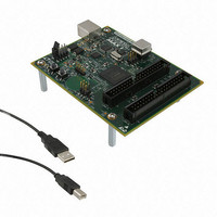
DK-DEV-5M570ZN Altera, DK-DEV-5M570ZN Datasheet - Page 13

DK-DEV-5M570ZN
Manufacturer Part Number
DK-DEV-5M570ZN
Description
KIT DEV MAX V 5M570Z
Manufacturer
Altera
Series
MAX® Vr
Type
CPLDr
Datasheets
1.DK-DEV-5M570ZN.pdf
(30 pages)
2.DK-DEV-5M570ZN.pdf
(2 pages)
3.DK-DEV-5M570ZN.pdf
(30 pages)
4.DK-DEV-5M570ZN.pdf
(164 pages)
5.DK-DEV-5M570ZN.pdf
(24 pages)
Specifications of DK-DEV-5M570ZN
Contents
Board, Cable(s), Software and Documentation
Silicon Manufacturer
Altera
Core Architecture
CPLD
Core Sub-architecture
MAX
Silicon Core Number
5M
Silicon Family Name
MAX V
Kit Contents
MAX V CPLD Development Board, USB Cable
Rohs Compliant
Yes
Lead Free Status / RoHS Status
Lead free / RoHS Compliant
For Use With/related Products
5M570ZF256
Lead Free Status / Rohs Status
Compliant
Other names
544-2722
Available stocks
Company
Part Number
Manufacturer
Quantity
Price
MV51002-1.0
Functional Description
© 2010 Altera Corporation. All rights reserved. ALTERA, ARRIA, CYCLONE, HARDCOPY, MAX, MEGACORE, NIOS, QUARTUS and STRATIX are Reg. U.S. Pat. & Tm. Off.
and/or trademarks of Altera Corporation in the U.S. and other countries. All other trademarks and service marks are the property of their respective holders as described at
www.altera.com/common/legal.html. Altera warrants performance of its semiconductor products to current specifications in accordance with Altera’s standard warranty, but
reserves the right to make changes to any products and services at any time without notice. Altera assumes no responsibility or liability arising out of the application or use of any
information, product, or service described herein except as expressly agreed to in writing by Altera. Altera customers are advised to obtain the latest version of device
specifications before relying on any published information and before placing orders for products or services.
MAX V Device Handbook
December 2010
This chapter describes the architecture of the MAX
following sections:
■
■
■
■
■
■
■
■
■
MAX V devices contain a two-dimensional row- and column-based architecture to
implement custom logic. Row and column interconnects provide signal interconnects
between the logic array blocks (LABs).
Each LAB in the logic array contains 10 logic elements (LEs). An LE is a small unit of
logic that provides efficient implementation of user logic functions. LABs are grouped
into rows and columns across the device. The MultiTrack interconnect provides fast
granular timing delays between LABs. The fast routing between LEs provides
minimum timing delay for added levels of logic versus globally routed interconnect
structures.
The I/O elements (IOEs) located after the LAB rows and columns around the
periphery of the MAX V device feeds the I/O pins. Each IOE contains a bidirectional
I/O buffer with several advanced features. I/O pins support Schmitt trigger inputs
and various single-ended standards, such as 33-MHz, 32-bit PCI™, and LVTTL.
MAX V devices provide a global clock network. The global clock network consists of
four global clock lines that drive throughout the entire device, providing clocks for all
resources within the device. You can also use the global clock lines for control signals
such as clear, preset, or output enable.
“Functional Description” on page 2–1
“Logic Array Blocks” on page 2–4
“Logic Elements” on page 2–8
“MultiTrack Interconnect” on page 2–14
“Global Signals” on page 2–19
“User Flash Memory Block” on page 2–21
“Internal Oscillator” on page 2–22
“Core Voltage” on page 2–25
“I/O Structure” on page 2–26
2. MAX V Architecture
®
V device and contains the
Subscribe


