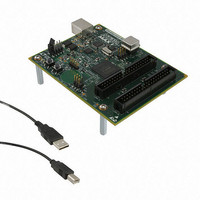
DK-DEV-5M570ZN Altera, DK-DEV-5M570ZN Datasheet - Page 25

DK-DEV-5M570ZN
Manufacturer Part Number
DK-DEV-5M570ZN
Description
KIT DEV MAX V 5M570Z
Manufacturer
Altera
Series
MAX® Vr
Type
CPLDr
Datasheets
1.DK-DEV-5M570ZN.pdf
(30 pages)
2.DK-DEV-5M570ZN.pdf
(2 pages)
3.DK-DEV-5M570ZN.pdf
(30 pages)
4.DK-DEV-5M570ZN.pdf
(164 pages)
5.DK-DEV-5M570ZN.pdf
(24 pages)
Specifications of DK-DEV-5M570ZN
Contents
Board, Cable(s), Software and Documentation
Silicon Manufacturer
Altera
Core Architecture
CPLD
Core Sub-architecture
MAX
Silicon Core Number
5M
Silicon Family Name
MAX V
Kit Contents
MAX V CPLD Development Board, USB Cable
Rohs Compliant
Yes
Lead Free Status / RoHS Status
Lead free / RoHS Compliant
For Use With/related Products
5M570ZF256
Lead Free Status / Rohs Status
Compliant
Other names
544-2722
Available stocks
Company
Part Number
Manufacturer
Quantity
Price
Chapter 2: MAX V Architecture
Logic Elements
December 2010 Altera Corporation
LE RAM
f
The Quartus II software automatically creates carry chain logic during design
processing, or you can create it manually during design entry. Parameterized
functions such as LPM functions automatically take advantage of carry chains for the
appropriate functions. The Quartus II software creates carry chains longer than 10 LEs
by linking adjacent LABs within the same row together automatically. A carry chain
can extend horizontally up to one full LAB row, but does not extend between LAB
rows.
Clear and Preset Logic Control
LAB-wide signals control the logic for the register’s clear and preset signals. The LE
directly supports an asynchronous clear and preset function. The register preset is
achieved through the asynchronous load of a logic high. MAX V devices support
simultaneous preset/asynchronous load and clear signals. An asynchronous clear
signal takes precedence if both signals are asserted simultaneously. Each LAB
supports up to two clears and one preset signal.
In addition to the clear and preset ports, MAX V devices provide a chip-wide reset pin
(DEV_CLRn) that resets all registers in the device. An option set before compilation in
the Quartus II software controls this pin. This chip-wide reset overrides all other
control signals and uses its own dedicated routing resources without using any of the
four global resources. Driving this signal low before or during power-up prevents
user mode from releasing clears within the design. This allows you to control when
clear is released on a device that has just been powered-up. If not set for its chip-wide
reset function, the DEV_CLRn pin is a regular I/O pin.
By default, all registers in MAX V devices are set to power-up low. However, this
power-up state can be set to high on individual registers during design entry using
the Quartus II software.
The Quartus II memory compiler can configure the unused LEs as LE RAM.
MAX V devices support the following memory types:
■
■
■
■
■
■
For more information about memory, refer to the
User
FIFO synchronous R/W
FIFO asynchronous R/W
1 port SRAM
2 port SRAM
3 port SRAM
shift registers
Guide.
Internal Memory (RAM and ROM)
MAX V Device Handbook
2–13


