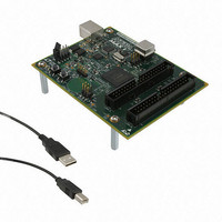
DK-DEV-5M570ZN Altera, DK-DEV-5M570ZN Datasheet - Page 120

DK-DEV-5M570ZN
Manufacturer Part Number
DK-DEV-5M570ZN
Description
KIT DEV MAX V 5M570Z
Manufacturer
Altera
Series
MAX® Vr
Type
CPLDr
Datasheets
1.DK-DEV-5M570ZN.pdf
(30 pages)
2.DK-DEV-5M570ZN.pdf
(2 pages)
3.DK-DEV-5M570ZN.pdf
(30 pages)
4.DK-DEV-5M570ZN.pdf
(164 pages)
5.DK-DEV-5M570ZN.pdf
(24 pages)
Specifications of DK-DEV-5M570ZN
Contents
Board, Cable(s), Software and Documentation
Silicon Manufacturer
Altera
Core Architecture
CPLD
Core Sub-architecture
MAX
Silicon Core Number
5M
Silicon Family Name
MAX V
Kit Contents
MAX V CPLD Development Board, USB Cable
Rohs Compliant
Yes
Lead Free Status / RoHS Status
Lead free / RoHS Compliant
For Use With/related Products
5M570ZF256
Lead Free Status / Rohs Status
Compliant
Other names
544-2722
Available stocks
Company
Part Number
Manufacturer
Quantity
Price
7–18
MAX V Device Handbook
The ALTUFM_I2C megafunction supports four different erase operation methods
shown on page 4 of the ALTUFM MegaWizard Plug-In Manager:
■
■
■
■
These erase options only work as described if that particular option is selected in the
MegaWizard Plug-In Manager before compiling the design files and programming
the device. Only one option can be selected for the ALTUFM_I2C megafunction.
Each erase option is discussed in more detail in the following sections.
Full Erase (Device Slave Address Triggered)
The full erase option uses the A
between an erase or read/write operation. This slave operation decoding occurs when
the master transfers the slave address to the slave after generating the start condition.
If the A
the four remaining MSBs match the rest of the slave addresses, then the Full Erase
operation is selected. If the A
to the UFM match its unique slave address setting, the read/write operation is
selected and functions as expected. As a result, this erase option utilizes two slave
addresses on the bus reserving A
of the UFM block will be erased when the Full Erase operation is executed. This
operation requires acknowledge polling. The internal UFM erase function only begins
after the master generates a stop condition.
triggered by using the slave address.
If the memory is write-protected (WP = 1), the slave does not acknowledge the erase
trigger slave address (A
then send a stop condition to terminate the transfer. The full erase operation will not
be executed.
Figure 7–13. Full Erase Sequence Triggered Using the Slave Address
Full Erase (Device Slave Address Triggered)
Sector Erase (Byte Address Triggered)
Sector Erase (A
No Erase
2
, A
1
, and A
2
0
S – Start Condition
P – Stop Condition
A – Acknowledge
Triggered)
slave address bits transmitted to the UFM slave equals 111 and
S
6
, A
Slave Address
A
5
, A
6
6
A
, A
5
A
4
2
, A
4
, A
5
A
6
, A
, A
3
111
3
1
, 1, 1, 1) sent by the master. The master should
4
, A
, A
5
, A
'0' (write)
0
3
bits of the slave address to distinguish
4
A
R/W
, A
2
, A
Figure 7–13
3
, 1, 1, 1 as the erase trigger. Both sectors
1
A
, and A
Chapter 7: User Flash Memory in MAX V Devices
P
From Master to Slave
From Slave to Master
0
slave address bits transmitted
shows the full erase sequence
January 2011 Altera Corporation
Software Support for UFM Block


