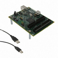
DK-DEV-5M570ZN Altera, DK-DEV-5M570ZN Datasheet - Page 113

DK-DEV-5M570ZN
Manufacturer Part Number
DK-DEV-5M570ZN
Description
KIT DEV MAX V 5M570Z
Manufacturer
Altera
Series
MAX® Vr
Type
CPLDr
Datasheets
1.DK-DEV-5M570ZN.pdf
(30 pages)
2.DK-DEV-5M570ZN.pdf
(2 pages)
3.DK-DEV-5M570ZN.pdf
(30 pages)
4.DK-DEV-5M570ZN.pdf
(164 pages)
5.DK-DEV-5M570ZN.pdf
(24 pages)
Specifications of DK-DEV-5M570ZN
Contents
Board, Cable(s), Software and Documentation
Silicon Manufacturer
Altera
Core Architecture
CPLD
Core Sub-architecture
MAX
Silicon Core Number
5M
Silicon Family Name
MAX V
Kit Contents
MAX V CPLD Development Board, USB Cable
Rohs Compliant
Yes
Lead Free Status / RoHS Status
Lead free / RoHS Compliant
For Use With/related Products
5M570ZF256
Lead Free Status / Rohs Status
Compliant
Other names
544-2722
Available stocks
Company
Part Number
Manufacturer
Quantity
Price
- DK-DEV-5M570ZN PDF datasheet
- DK-DEV-5M570ZN PDF datasheet #2
- DK-DEV-5M570ZN PDF datasheet #3
- DK-DEV-5M570ZN PDF datasheet #4
- DK-DEV-5M570ZN PDF datasheet #5
- Current page: 113 of 164
- Download datasheet (5Mb)
Chapter 7: User Flash Memory in MAX V Devices
UFM Operating Modes
January 2011 Altera Corporation
Erase
1
The ERASE signal initiates an erase sequence to erase one sector of the UFM. The data
register is not needed to perform an erase sequence. To indicate the sector of the UFM
to be erased, the MSB of the address register should be loaded with 0 to erase UFM
sector 0, or 1 to erase UFM sector 1
ERASE signal, the memory sector indicated by the MSB of the address register will be
erased. The BUSY signal is asserted until the erase sequence is completed. The address
register should not be modified until the BUSY signal is de-asserted to prevent the flash
content from being corrupted. This ERASE signal is ignored when the BUSY signal is
asserted.
When the UFM sector is erased, it has 16-bit locations all filled with FFFF. Each UFM
storage bit can be programmed only once between erase sequences. You can write to
any word up to two times providing the second programming attempt at that location
only adds 0s. 1s are mask bits for your input word that cannot overwrite 0s in the
flash array. New 1s in the location can only be achieved by an erase. Therefore, it is
possible for you to perform byte writes because the UFM array is 16 bits for each
location.
Figure 7–8. UFM Erase Waveforms
Figure 7–8
PROGRAM
OSC_ENA
DRSHFT
ARSHFT
DRDout
DRCLK
ERASE
ARCLK
ARDin
DRDin
BUSY
illustrates the UFM waveforms during erase mode.
t
t
ASU
ADS
t
ACLK
(Figure 7–2 on page
9 Address Bits
t
ADH
t
AH
t
EB
t
OSCS
7–5). On a rising edge of the
t
EPMX
t
OSCH
t
MAX V Device Handbook
BE
7–11
Related parts for DK-DEV-5M570ZN
Image
Part Number
Description
Manufacturer
Datasheet
Request
R

Part Number:
Description:
KIT DEV ARRIA II GX FPGA 2AGX125
Manufacturer:
Altera
Datasheet:

Part Number:
Description:
KIT DEV CYCLONE III LS EP3CLS200
Manufacturer:
Altera
Datasheet:

Part Number:
Description:
KIT DEV STRATIX IV FPGA 4SE530
Manufacturer:
Altera
Datasheet:

Part Number:
Description:
KIT DEV FPGA 2AGX260 W/6.375G TX
Manufacturer:
Altera
Datasheet:

Part Number:
Description:
KIT DEV STRATIX V FPGA 5SGXEA7
Manufacturer:
Altera
Datasheet:

Part Number:
Description:
KIT DEVELOPMENT STRATIX III
Manufacturer:
Altera
Datasheet:

Part Number:
Description:
KIT DEVELOPMENT STRATIX IV
Manufacturer:
Altera
Datasheet:

Part Number:
Description:
KIT DEV ARRIA GX 1AGX60N
Manufacturer:
Altera
Datasheet:

Part Number:
Description:
KIT STARTER CYCLONE IV GX
Manufacturer:
Altera
Datasheet:

Part Number:
Description:
KIT DEVELOPMENT STRATIX IV
Manufacturer:
Altera
Datasheet:

Part Number:
Description:
CPLD, EP610 Family, ECMOS Process, 300 Gates, 16 Macro Cells, 16 Reg., 16 User I/Os, 5V Supply, 35 Speed Grade, 24DIP
Manufacturer:
Altera Corporation
Datasheet:

Part Number:
Description:
CPLD, EP610 Family, ECMOS Process, 300 Gates, 16 Macro Cells, 16 Reg., 16 User I/Os, 5V Supply, 15 Speed Grade, 24DIP
Manufacturer:
Altera Corporation
Datasheet:


